Semiconductor device and fabrication method thereof

a technology of semiconductor devices and semiconductor wafers, applied in the direction of basic electric elements, color television, television systems, etc., can solve the problems of affecting the top surface of the covering layer onto which light is incident, limiting the yield of semiconductor devices obtained from one semiconductor wafer, etc., to achieve the effect of reducing the thickness avoiding damage to the semiconductor wafer, and maintaining the strength of the semiconductor wafer

Inactive Publication Date: 2010-02-04
LAPIS SEMICON CO LTD
View PDF3 Cites 50 Cited by
  • Summary
  • Abstract
  • Description
  • Claims
  • Application Information

AI Technical Summary

Benefits of technology

[0032]Since the process for forming the bonded body of the light transmitting substrate and the semiconductor wafer, includes a process of grinding away the semiconductor wafer and reducing the thickness of the semiconductor waf...

Problems solved by technology

Also, in comparison to when a blade appropriate to a covering layer is used, with a blade appropriate for both materials there is concern of breakage and defects etc. occurring at the cut face of the covering layer and also of affecting the top surface of the covering layer onto which light is incident.
When the side surfaces of a semiconductor device are cut at an angle this also limits the yield of semiconductor devices obtained from one semiconductor wafer.
However, since light enters from the side surfaces of the above cover glass, there is the problem that desired characteristics are not obtained.
In addition, the cover glass and the semiconductor wafer are partitioned using dicing technology, requiring a wide cut width by a blade suited to both materials, and therefore the ...

Method used


Image

  • Semiconductor device and fabrication method thereof
  • Semiconductor device and fabrication method thereof
  • Semiconductor device and fabrication method thereof

Examples


Embodiment Construction

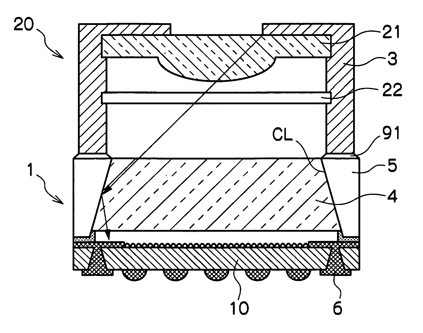
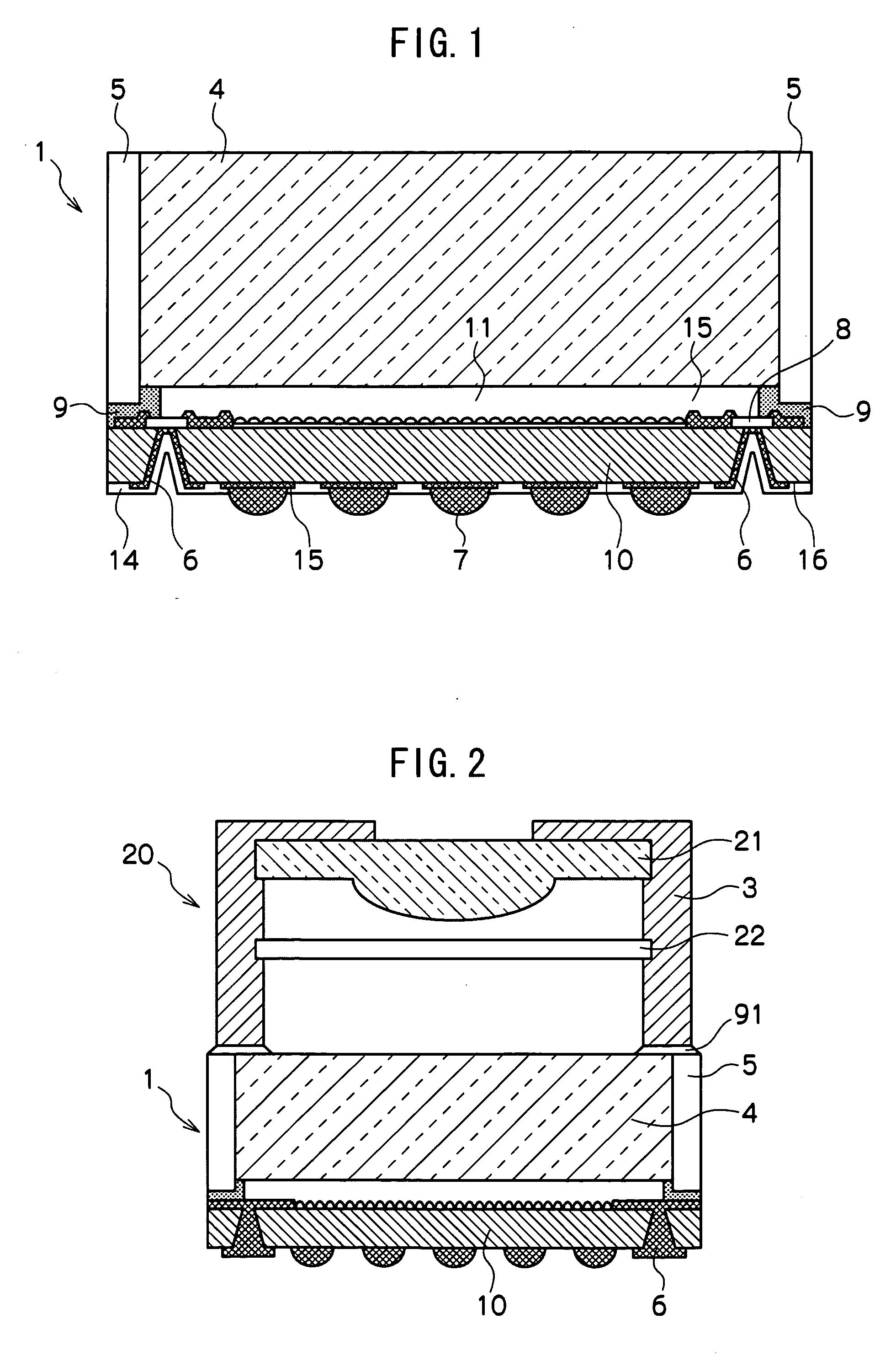
[0053]Explanation will now be given regarding details of a sensor module of a semiconductor device of an exemplary embodiment of the present invention, with reference to the attached drawings. It should be noted that in each of the drawings, where the same configuration element is shown in separate drawings the same reference number is allocated thereto, and detailed explanation thereof is omitted.

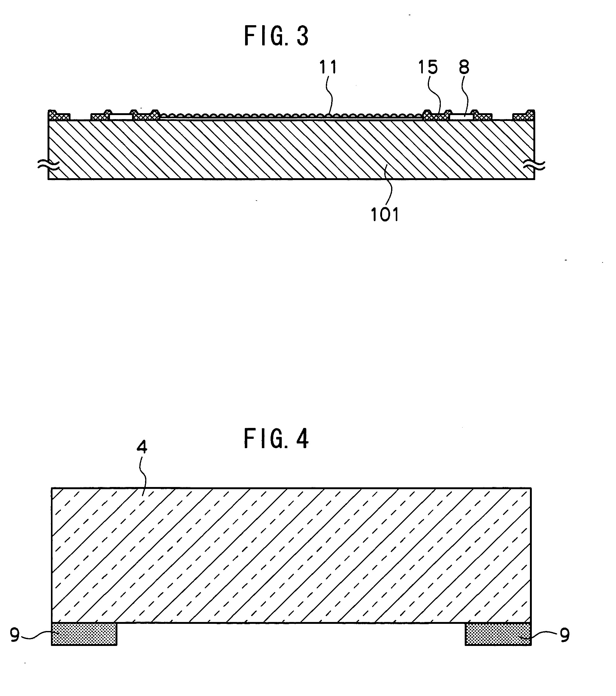
[0054]FIG. 1 is a cross-section of a sensor module of a first exemplary embodiment. A sensor module 1 is configured overall including a glass plate 4 that is a light transmitting chip, and a semiconductor chip 10, formed from silicon or the like, to which the glass plate 4 is attached by a bonding layer 9. A UV-curable or heat-curable material is employed as the material of the bonding layer 9.

[0055]A light blocking resin layer 5 is formed on the bonding layer 9, stuck onto the side surfaces of the glass plate 4.

[0056]A photoreceptor portion 11 including photoreceptor elements, such as CMO...


PUM


Abstract

There is provided a semiconductor device including: a semiconductor chip having a penetrating electrode penetrating through from a first main surface of the semiconductor chip to a second main surface on the opposite side thereof, a photoreceptor portion formed on the first main surface, and a first wire at a periphery of the photoreceptor portion; a light transmitting chip adhered to the first main surface at the periphery of the light transmitting chip, with a bonding layer interposed between the light transmitting chip and the first main surface, the light transmitting chip covering the light transmitting chip; and a light blocking resin layer formed only on the side surfaces of the light transmitting chip and the bonding layer.

Description

CROSS-REFERENCE TO RELATED APPLICATION[0001]This application claims priority under 35 USC 119 from Japanese Patent Application No. 2008-200010 filed on Aug. 1, 2008, the disclosure of which is incorporated by reference herein.BACKGROUND[0002]1. Technical Field[0003]The present invention relates to a semiconductor device and to a fabrication method thereof. In particular the present invention relates to a semiconductor device structure having a semiconductor chip, such as a sensor module, and a protection glass.[0004]2. Related Art[0005]Existing known semiconductor devices having a semiconductor chip, such as a sensor module, and a protection glass include: a structure with a light blocking film formed on the side surfaces of an optical member provided on microlenses of a semiconductor chip (see Japanese Patent Application Laid-Open (JP-A) No. 2007-142058); a structure having a covering layer formed on a semiconductor chip having a circuit portion including a photoreceptor element, w...

Claims


Application Information

Patent Timeline
IPC IPC(8): H01L33/00H01L23/02H01L23/06H01L27/14H01L31/02H04N5/335H04N5/357H04N5/369
CPCH01L27/14618H01L27/14621H04N5/2257H01L31/0203H01L27/14627H01L2224/13H01L2224/05009H01L2224/05548H01L2224/0557H01L2224/05001H01L2224/05624H01L2224/05639H01L2224/05644H01L2224/05647H01L2224/05655H01L2924/00014H01L24/05H01L2224/02377H04N23/57H01L2224/05599H01L2224/05099
Inventor YAMADA, SHIGERUTERUI, MAKOTOEGAWA, YOSHIMIOHUCHI, SHINJI
Owner LAPIS SEMICON CO LTD
Why Eureka
Try Eureka