Microstrip array antenna
- Summary
- Abstract
- Description
- Claims
- Application Information
AI Technical Summary
Benefits of technology
Problems solved by technology
Method used
Image

Examples
first embodiment
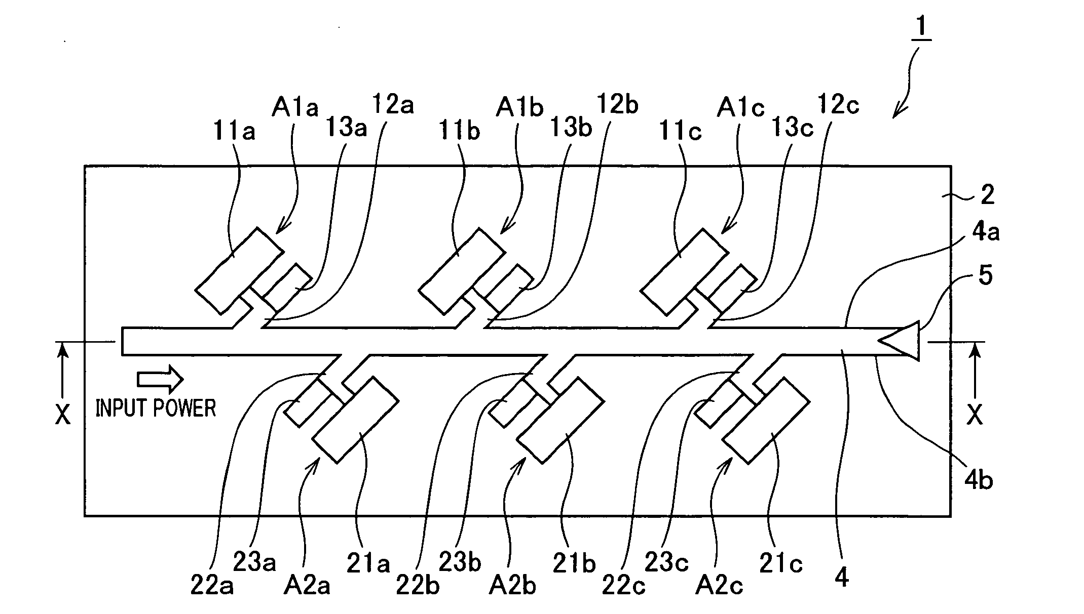
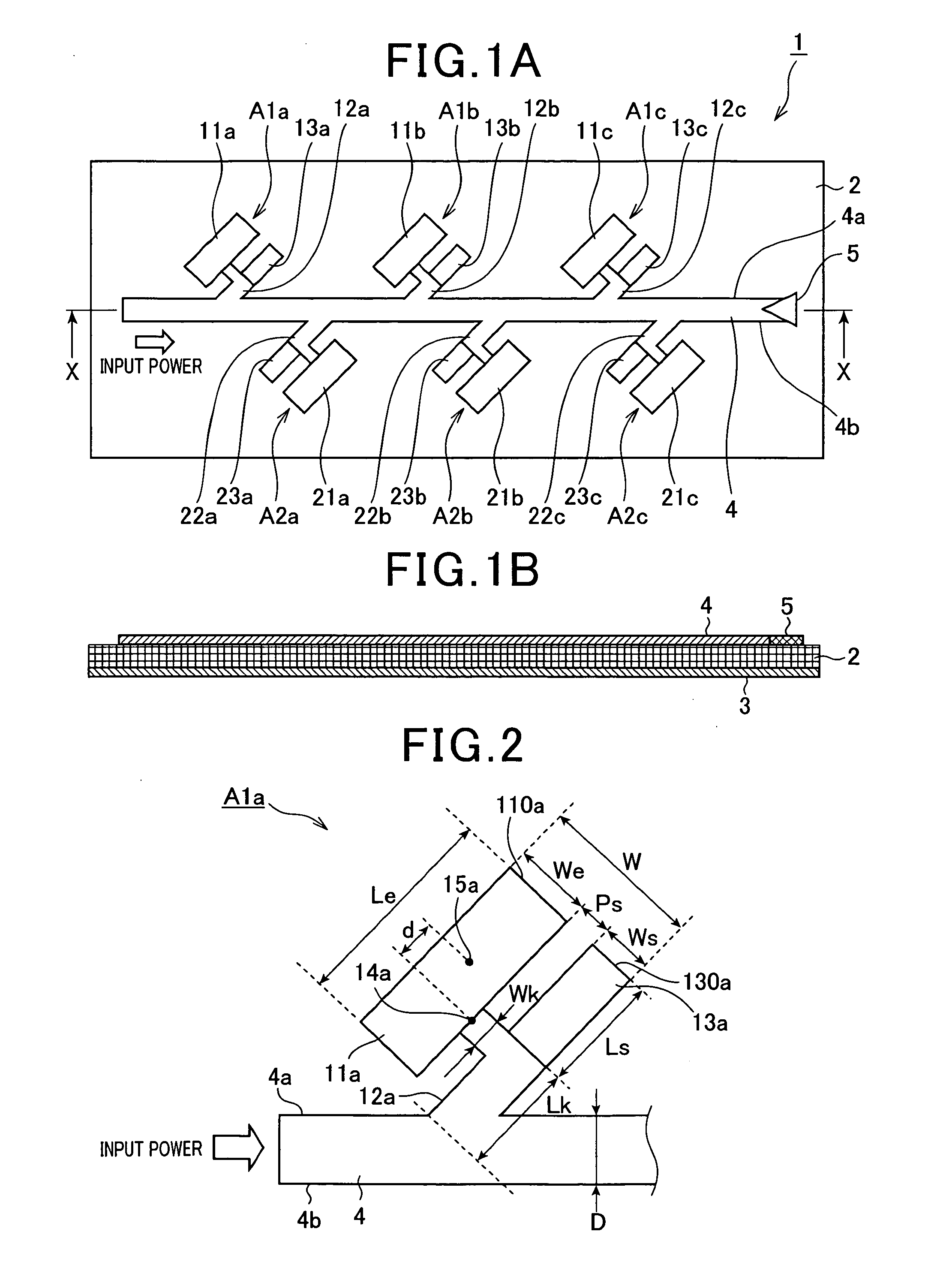
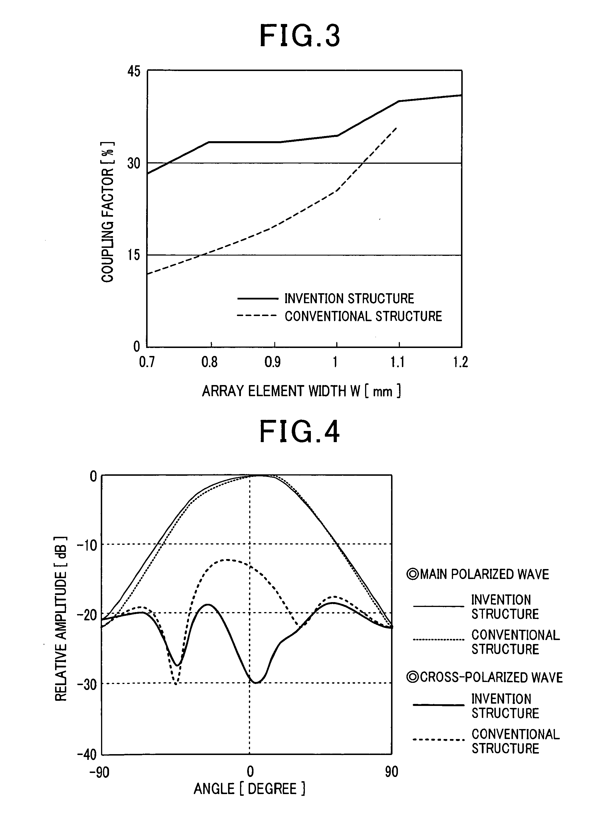
[0054]FIG. 1A is a plan view of a microstrip array antenna 1 according to a first embodiment of the invention. FIG. 1B is a cross-sectional view of the microstrip array antenna 1 taken along the line X-X in FIG. 1A.
[0055]The microstrip array antenna 1 is constituted of strip conductors formed on a front surface of a dielectric substrate 2 formed with a conductive ground plate 3 at its back surface. As shown in FIG. 1A, the strip conductors on the front surface of the dielectric substrate 2 includes a linearly disposed main feeding strip line 4, and a plurality of array elements A1a, A1b, A1c, A2a, A2b and A2c connected to either side edge of the main feeding strip line 4.
[0056]In more detail, the array elements A1a, A1b and A1c are connected to a first side edge 4a (one of two side edges of the main feeding strip line 4) at a predetermined interval therebetween. This predetermined interval is equal to the wavelength λg of a radio wave propagating the strip conductors at an operating...
second embodiment
[0115]Next, a microstrip array antenna 30 according to a second embodiment of the invention is described with respect to FIG. 11.
[0116]The microstrip array antenna 30 according to the second embodiment of the invention has a structure in which array elements A3a, A3b, A3c, A4a, A4b and A4c are connected to either side edge of the main feeding strip line 4. The number of the array elements connected to the main feeding strip line 4 and the connection interval are the same like the first embodiment.
[0117]The array element A3a, which is the closest of the array elements connected to the first side edge 4a of the main feeding strip line 4 to the input end, is constituted of a sub-feeding strip line 32a connected to the main feeding strip line 4, a rectangular radiating antenna element 31a connected to the terminal end of the sub-feeding strip line 32a, and a stub 33a connected to a predetermined middle portion of the sub-feeding strip line 32a.
[0118]Likewise, the array element A3b, whi...
PUM
 Abstract
Description
Claims
Application Information
 - Generate Ideas
- Intellectual Property
- Life Sciences
- Materials
- Tech Scout
- Unparalleled Data Quality
- Higher Quality Content
- 60% Fewer Hallucinations
Browse by: Latest US Patents, China's latest patents, Technical Efficacy Thesaurus, Application Domain, Technology Topic, Popular Technical Reports.
© 2025 PatSnap. All rights reserved.Legal|Privacy policy|Modern Slavery Act Transparency Statement|Sitemap|About US| Contact US: help@patsnap.com