Susceptor, vapor phase growth apparatus, and method of manufacturing epitaxial wafer

a technology of vapor phase growth and substrate, which is applied in the direction of polycrystalline material growth, chemically reactive gas growth, crystal growth process, etc., can solve the problem of difficulty in raising the surface use rate, and achieve good crystallinity and reduce the defect of semiconductor elements

Inactive Publication Date: 2010-02-04
SUMCO CORP
View PDF9 Cites 40 Cited by
  • Summary
  • Abstract
  • Description
  • Claims
  • Application Information

AI Technical Summary

Benefits of technology

[0021]Since a non-limiting feature of the present invention permits the formation of an epitaxial layer of good crystallinity on a semiconductor wafer, it is possible to reduce the crystal defects in a semiconductor element based on the crystal orientation of a semiconductor wafer, particularly crystal defects on or near the surface.

Problems solved by technology

The perimeter portions of such epitaxial wafers cannot be used to fabricate devices, making it difficult to raise the use rate in the surface.

Method used


Image

  • Susceptor, vapor phase growth apparatus, and method of manufacturing epitaxial wafer
  • Susceptor, vapor phase growth apparatus, and method of manufacturing epitaxial wafer
  • Susceptor, vapor phase growth apparatus, and method of manufacturing epitaxial wafer

Examples


example 1

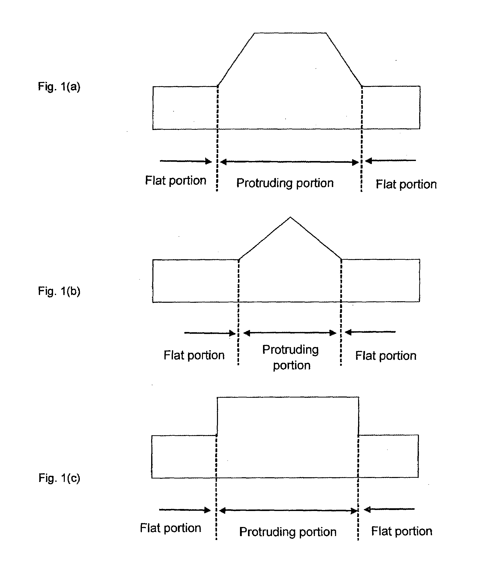
[0075]A 300 mm semiconductor wafer on which an epitaxial layer is to be formed on the (100) face thereof was placed on a susceptor that had been disposed within the reaction chamber of a vapor phase growth apparatus and that was equipped with protruding portions in the 85° to 95°, 175° to 185°, 265° to 275°, and 355° to 5° portions thereof when the position opposite the wafer notch (notch-opposing part) of the lateral wall of the counterbored groove was aligned with 0°.

[0076]An epitaxial film was grown by vapor phase epitaxy on the surface of the semiconductor wafer placed on the susceptor. The epitaxial growth process will be described in detail below.

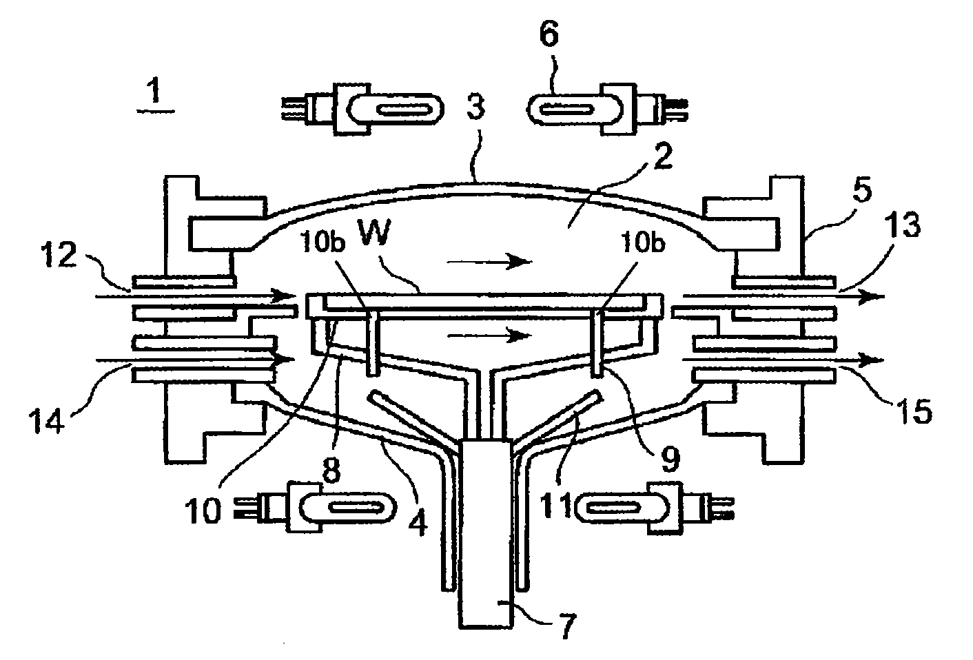
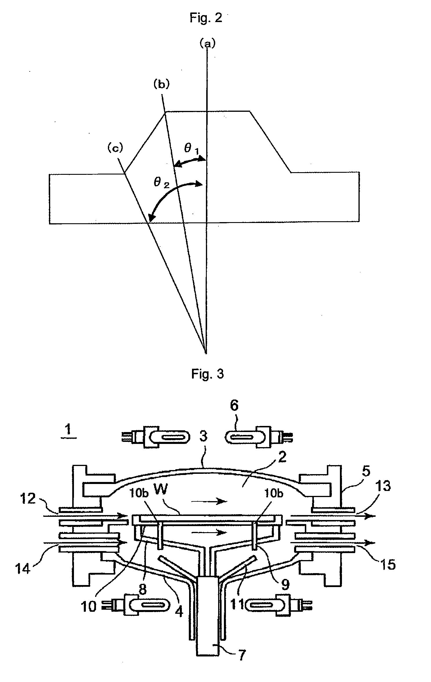
[0077]The vapor phase epitaxial growth apparatus employed comprised a chamber above and below which heaters were disposed, and in the center of which was horizontally disposed a susceptor that was capable of holding a single wafer and that was round when viewed from above.

[0078]An upper counterbored portion (annular difference in heig...


PUM

PropertyMeasurementUnit
heightaaaaaaaaaa
diameteraaaaaaaaaa
angle θ1aaaaaaaaaa

Abstract

An aspect of the present invention relates to a susceptor comprising a counterbored groove receiving a semiconductor wafer in the course of manufacturing an epitaxial wafer by vapor phase growing an epitaxial layer on a surface of the semiconductor wafer, wherein a lateral wall of the counterbored groove is comprised of at least one flat portion and at least one protruding portion being higher than the flat portion, and a height of the flat portion is equal to or greater than a thickness of the semiconductor wafer.

Description

CROSS-REFERENCE TO RELATED APPLICATIONS[0001]This application claims the benefit of priority under 35 USC 119 to Japanese Patent Application No. 2008-197880, filed on Jul. 31, 2008, which is expressly incorporated herein by reference in its entirety.BACKGROUND OF THE INVENTION[0002]1. Field of the Invention[0003]The present invention relates to a susceptor and a vapor phase growth apparatus, and more particularly, to a susceptor permitting the manufacturing of an epitaxial wafer comprising an epitaxial layer of uniform thickness, and to a vapor phase growth apparatus comprising the susceptor.[0004]The present invention further relates to a method of manufacturing an epitaxial wafer employing the above susceptor.[0005]2. Discussion of the Background of the Invention[0006]The reduction of crystal defects in semiconductors, particularly crystal defects on or near the surface, has been gaining importance in recent years with the high level of integration of semiconductor devices. Thus, ...

Claims


Application Information

Patent Timeline
Patent Type & Authority Applications(United States)
IPC IPC(8): H01L21/36C23C16/458
CPCC23C16/4584C23C16/4585C30B25/12H01L21/67386H01L21/02532H01L21/0262C30B29/06
Inventor MIYASHITA, JUNJI
Owner SUMCO CORP
Why Eureka
Try Eureka