Interlayer insulating film, wiring structure and electronic device and methods of manufacturing the same

a technology of interlayer insulating film and wiring structure, which is applied in the direction of semiconductor devices, electrical equipment, semiconductor/solid-state device details, etc., can solve the problems of parasitic capacitance between wirings and wiring resistance becoming unavoidable, poor adhesion of cfx film, and low dielectric constant, so as to improve the other electric characteristics of cfx film, improve the dielectric breakdown voltage, and reduce the dielectric constant

Inactive Publication Date: 2010-02-11
TOHOKU UNIV +1
View PDF6 Cites 8 Cited by
  • Summary
  • Abstract
  • Description
  • Claims
  • Application Information

AI Technical Summary

Benefits of technology

[0008]On the other hand, in a wiring structure on the semiconductor element, in particular, in a wiring structure including an interlayer insulating film, it is required to further decrease the dielectric constant. However, no proposal has been made about further decrease of the dielectric constant of the CFx film as the interlayer insulating film. Also, in case where the CF film is used as the interlayer insulating film, it is desired to improve other electric characteristics of the CFx film, in particular, to improve a dielectric breakdown voltage and to reduce a leak current.

Problems solved by technology

In the above-mentioned multilayer wiring structure, a problem of signal delay due to a parasitic capacitance between wirings and a wiring resistance has becomes unavoidable.
However, the CFx film is very weak against water and poor in adhesion.

Method used


Image

  • Interlayer insulating film, wiring structure and electronic device and methods of manufacturing the same
  • Interlayer insulating film, wiring structure and electronic device and methods of manufacturing the same
  • Interlayer insulating film, wiring structure and electronic device and methods of manufacturing the same

Examples


embodiments

[0101]Now, embodiments of this invention will be described with reference to the drawing.

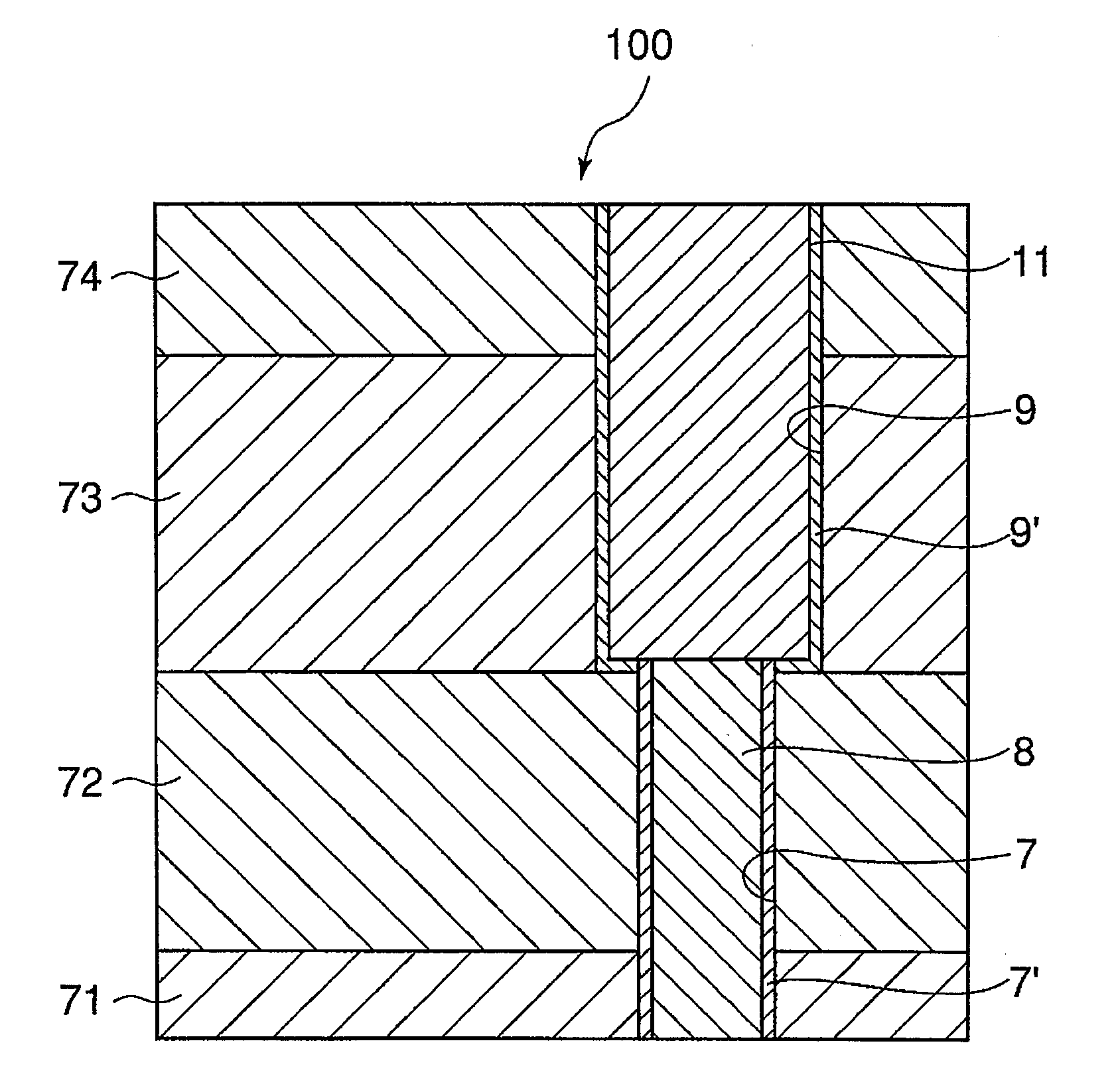
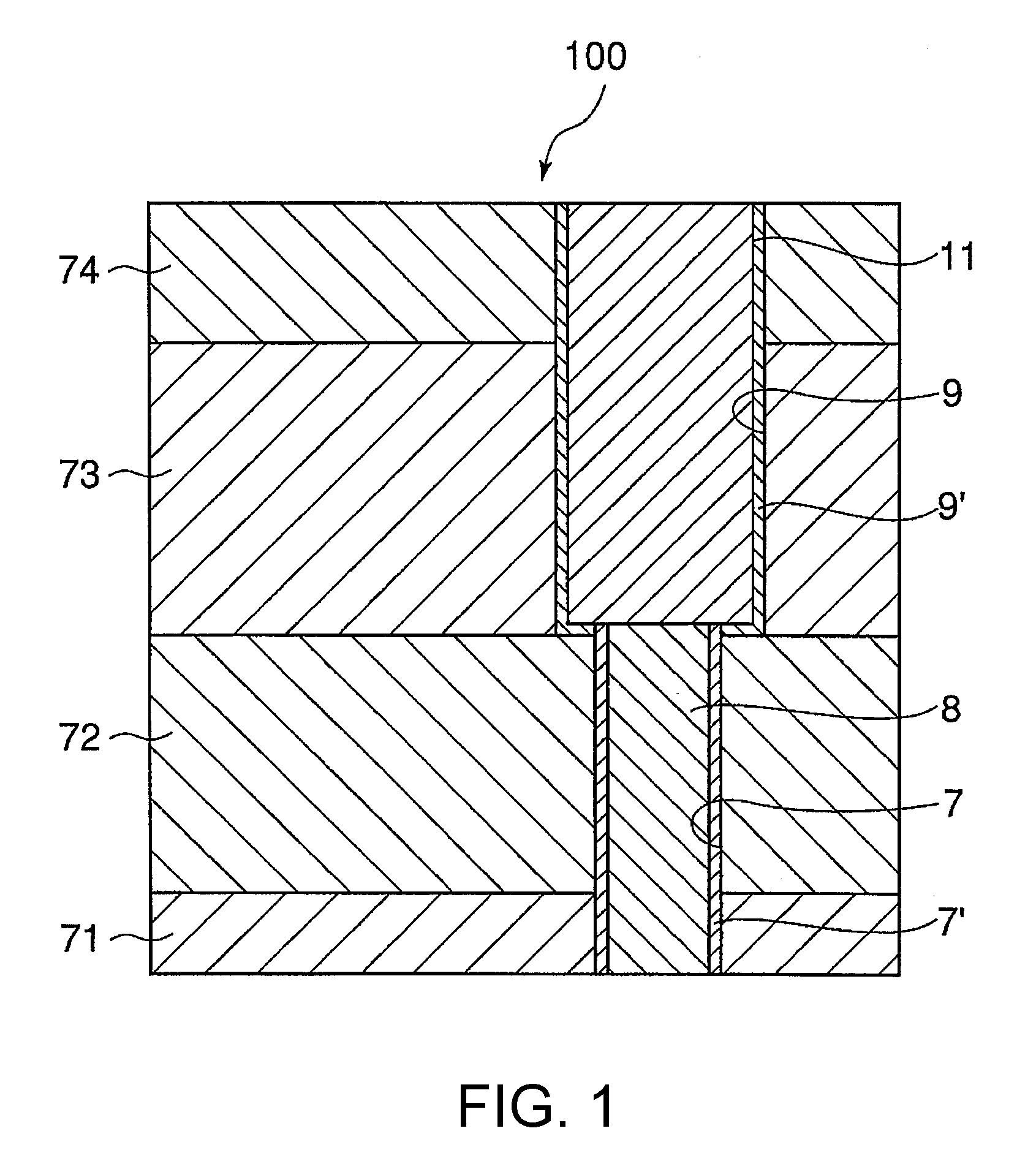
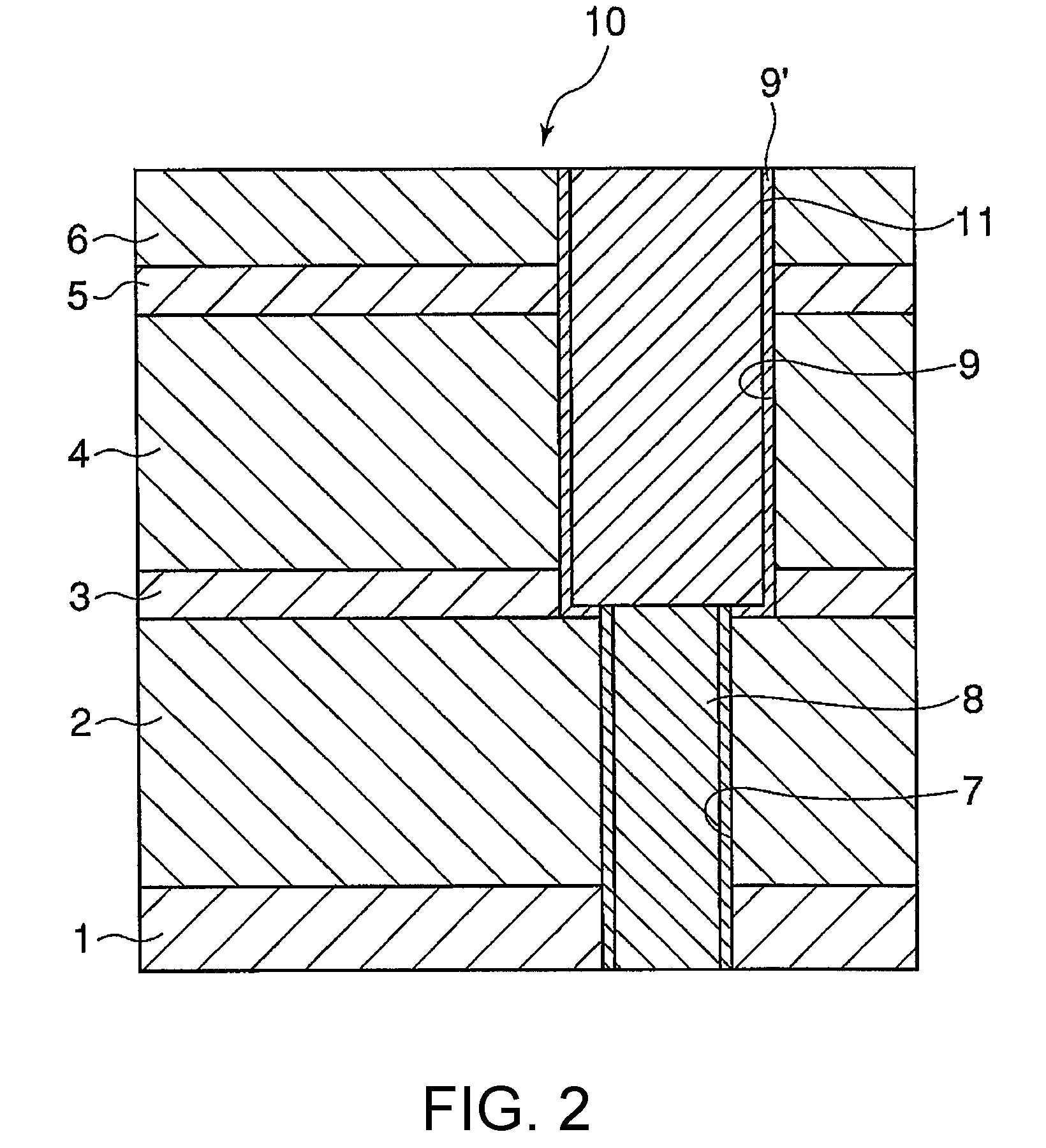
[0102]FIG. 2 is a sectional view showing a wiring structure according to an embodiment of this invention. As illustrated in FIG. 2, in a semiconductor device, a multilayer wiring structure (only one connecting portion between wiring layers is shown) 10 is formed on a semiconductor substrate (not shown) provided with a number of semiconductor elements. The multilayer wiring structure includes a barrier cap layer 1 of silicon carbonitride (SiCN) and an interlayer insulating film 2 formed thereon and comprising a fluorocarbon film (hereinafter referred to as a CFx film).

[0103]A via hole 7 is formed to penetrate the interlayer insulating film 2 and the barrier cap layer 1. An electrode or a wiring 8 of Cu is formed in the via hole 7. Furthermore, a second interlayer insulating film 4 comprising a fluorocarbon film is formed on the interlayer insulating film 2 through a first adhesive layer 3 of SiCN...


PUM


Abstract

A wiring structure of a semiconductor device or the like includes an interlayer insulating film having a fluorocarbon film formed on an underlayer, and a conductor buried in the interlayer insulating film. The fluorocarbon film contains nitrogen and is low in dielectric constant, excellent in reproducibility and stable.

Description

TECHNICAL FIELD[0001]This invention relates to a multilayer wiring or interconnection structure, particularly a structure of an interlayer insulating film, of a board or substrate, such as a semiconductor element, a semiconductor-chip mounting board or a wiring board, and further relates to a semiconductor device having the multilayer wiring structure, a wiring board having the multilayer wiring structure, and an electronic device including the same. This invention also relates to a method of manufacturing the multilayer wiring structure and methods of manufacturing the semiconductor device having the multilayer wiring structure, the wiring board having the multilayer wiring structure, and the electronic device including the same.BACKGROUND ART[0002]Heretofore, an interlayer insulating film is formed for the purpose of insulation between wiring layers in a multilayer wiring structure on a semiconductor substrate or the like.[0003]In the above-mentioned multilayer wiring structure, a...

Claims


Application Information

Patent Timeline
Patent Type & Authority Applications(United States)
IPC IPC(8): H01L23/48
CPCH01L21/0212H01L21/02274H01L21/02304H01L21/3127H01L21/76829H01L21/76835H01L2924/0002H01L21/76843H01L23/5329H01L23/53295H01L2924/00
Inventor OHMI, TADAHIROYASUDA, SEIJIINOKUCHI, ATSUTOSHIMATSUOKA, TAKAAKIKAWAMURA, KOHEI
Owner TOHOKU UNIV
Why Eureka
Try Eureka