Organic light emitting display device

a light-emitting display and organic technology, applied in the direction of instruments, static indicating devices, discharge tubes luminescnet screens, etc., can solve the problems of low light coupling efficiency of conventional oled devices, difficult manufacturing of optical structures, and small reproduction margins

Inactive Publication Date: 2010-02-11
SAMSUNG DISPLAY CO LTD
View PDF12 Cites 24 Cited by
  • Summary
  • Abstract
  • Description
  • Claims
  • Application Information

AI Technical Summary

Benefits of technology

[0011]According to another aspect of the present invention, there is provided an OLED device having an organic light emitting device that includes a first electrode and a second electrode facing each other, an organic light emitting layer arranged between the first electrode and the second electrode, wherein light emitted from the organic light emitting layer within an effective viewing angle range is transmitted along a first optical path and light emitted from the organic light emitting layer outside the effective viewing angle range is transmitted along a second optical path and a light scattering layer to allow the second optical path to pass therethrough and having an opening corresponding to the first optical path to prevent a main image transmitted along the first optical path from interfering with the light scattering layer. The light scattering layer can include a base including a transparent insulating material having a first refractive index and a plurality of fine particles including a material having a second refractive index that is higher than the first refractive index. The fine particles can be arranged within the base at a concentration of 5 to 50%. The fine particles can be one of titanium oxide, zirconium oxide and zinc oxide. The fine particles can have an average particle size of 50 to 500 nm.

Problems solved by technology

Accordingly, the conventional OLED device has the disadvantage of low light coupling efficiency due to its structural limitation.
However, such optical structures are difficult to manufacture and have small reproduction margins.
Also, conventional OLED devices have another disadvantage in that since internal light of one pixel leaks into adjacent pixels, color mixing between the pixels occurs.
In particular, if a photosensor is installed in each pixel, the photosensor can operate improperly due to the leakage of internal light.

Method used


Image

  • Organic light emitting display device
  • Organic light emitting display device
  • Organic light emitting display device

Examples


Embodiment Construction

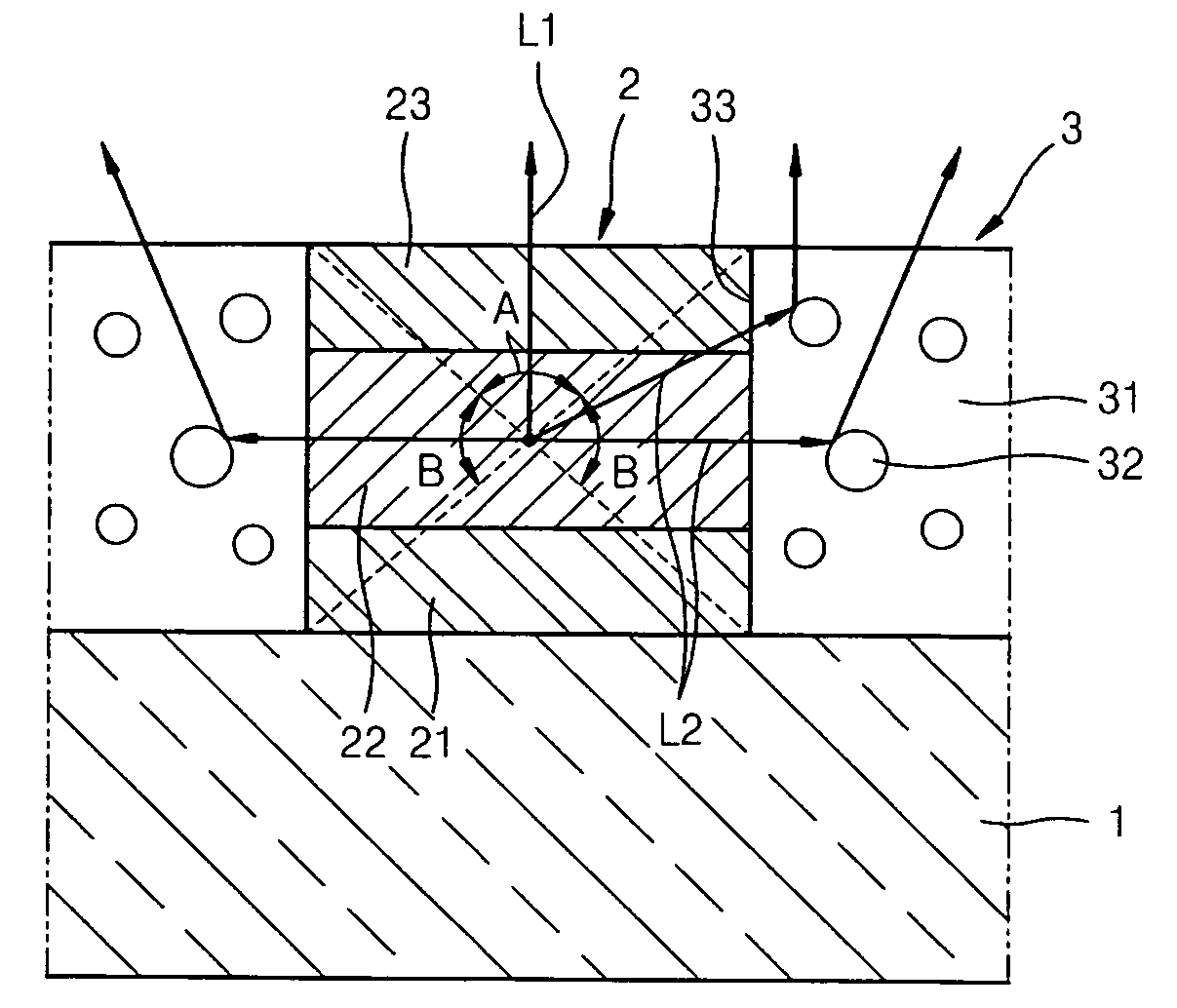
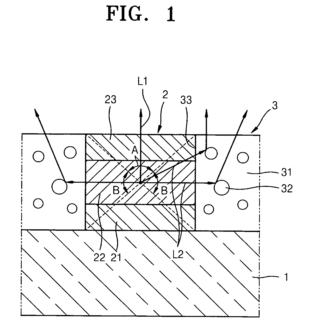
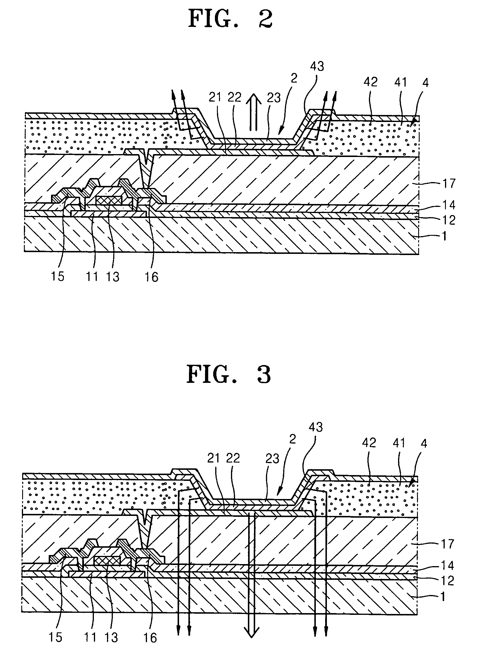
[0016]Turning now to FIG. 1, FIG. 1 is a cross-sectional view of an OLED device according to an embodiment of the present invention. Referring to FIG. 1, the OLED device includes an organic light emitting diode 2 and a light scattering layer 3 which are formed on a substrate 1. The organic light emitting diode 2 includes a first electrode 21 and a second electrode 23 which face each other, and an organic light emitting layer 22 arranged between the first electrode 21 and the second electrode 23. The first electrode 21 and the second electrode 23 can have opposite polarities, and thus can be an anode and a cathode, respectively, or vice versa.

[0017]The first electrode 21 and the second electrode 23 apply voltages of opposite polarities to the organic light emitting layer 22 arranged between the first electrode 21 and the second electrode 23 so that the organic light emitting layer 22 can emit light. The OLED device of FIG. 1 is a top emission OLED device where light is emitted away f...


PUM


Abstract

An organic light emitting display (OLED) device that can improve light coupling efficiency by causing laterally emitted light emitted from an organic light emitting layer to travel in a direction in which an image is formed, resulting in reduced color mixing between pixels by reducing the leakage of internal light. The OLED device includes a substrate, a first electrode arranged on the substrate, a light scattering layer arranged on the substrate and covering a portion of the first electrode and having an opening exposing a portion of the first electrode, a second electrode arranged on the light scattering layer and within the opening facing the first electrode and an organic light emitting layer arranged within the opening between the first electrode and the second electrode.

Description

CLAIM OF PRIORITY[0001]This application makes reference to, incorporates the same herein, and claims all benefits accruing under 35 U.S.C.§119 from an application for ORGANIC LIGHT EMITTING DISPLA4Y DEVICE earlier filed in the Korean Intellectual Property Office on 7 Aug. 2008 and there duly assigned Serial No. 10-2008-0077549.BACKGROUND OF THE INVENTION[0002]1. Field of the Invention[0003]The present invention relates to an organic light emitting display (OLED) device that can 1I improve light coupling efficiency and prevent color mixing between pixels.[0004]2. Description of the Related Art[0005]OLED devices are self-luminous display devices that emit light by electrically exciting an organic compound. OLED devices are drawing a great deal of attention as next generation display devices because of their low driving voltages, thin design, wide viewing angles, and fast response times which overcome the weaknesses of liquid crystal display (LCD) devices.[0006]However, in a convention...

Claims


Application Information

Patent Timeline
Patent Type & Authority Applications(United States)
IPC IPC(8): H01J1/62
CPCH01L27/3246H01L51/5268H01L27/3269H10K59/122H10K59/13H10K50/854G09G3/3473H01L2924/01022H01L2924/0104
Inventor LEE, SO-YOUNGLEE, JONG-HYUKLEE, SUN-YOUNGCHO, YOON-HYEUNGOH, MIN-HOLEE, BYOUNG DUK
Owner SAMSUNG DISPLAY CO LTD
Why Eureka
Try Eureka