Organic laser device

Active Publication Date: 2010-03-04
SEMICON ENERGY LAB CO LTD
View PDF32 Cites 16 Cited by
  • Summary
  • Abstract
  • Description
  • Claims
  • Application Information

AI Technical Summary

Benefits of technology

[0028]By applying one embodiment of the present invention, a small and lightweight sheet-shaped laser device which can be man

Problems solved by technology

However, the structure disclosed in Patent Document 1 requires complicated manufacturing steps: an organic EL element and a dye thin film having a distributed feedback resonator need to be formed on both sides of a glass substrate by adjusting the positions

Method used


Image

  • Organic laser device
  • Organic laser device
  • Organic laser device

Examples


embodiment 1

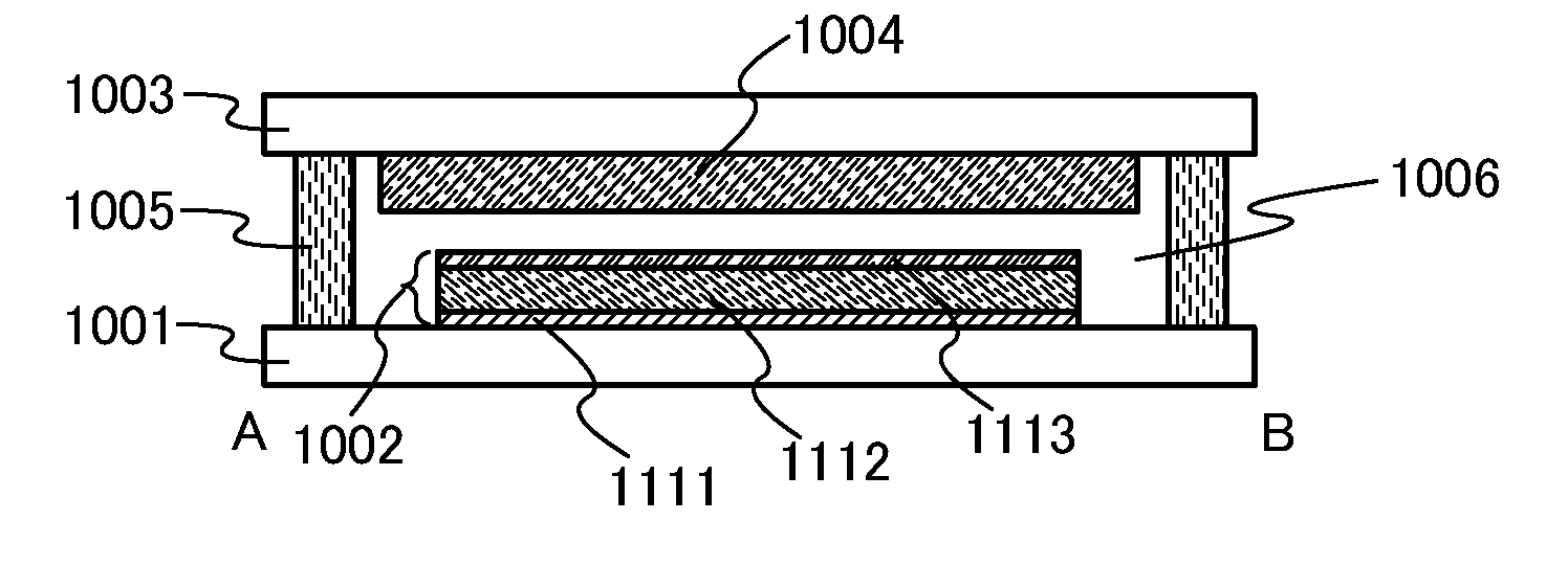
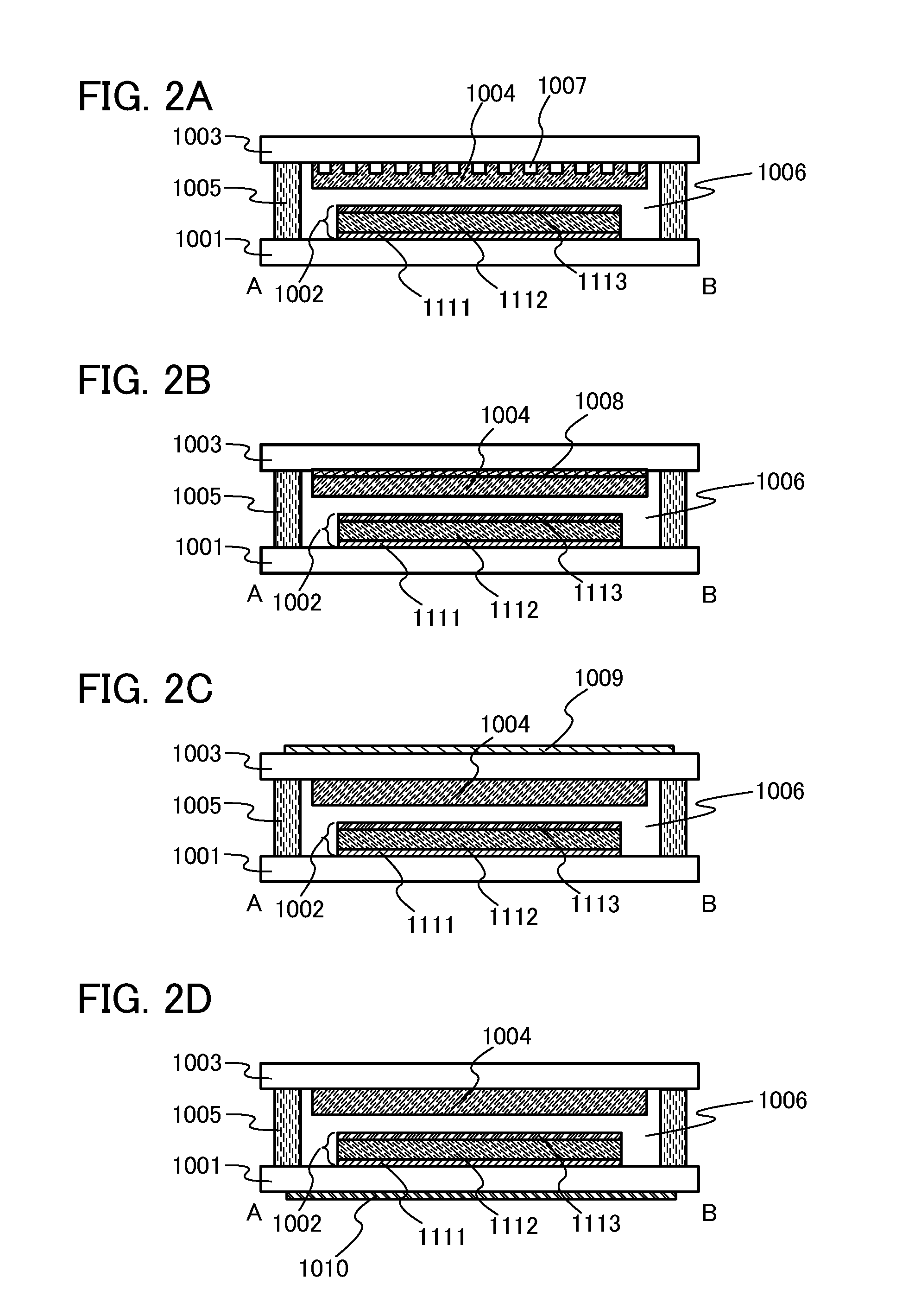
[0035]An organic laser device of this embodiment is a laser device with which a laser medium and a light source are integrated. A light-emitting element is used as the light source. The light-emitting element is a plane light source. Further, a film containing a laser dye as a laser medium is formed in a region facing the light source. An optical resonator is preferably provided with a substrate over which the film containing a laser dye as a laser medium is formed. The arrangement of the optical resonator over the laser medium is not particularly limited. The optical resonator may be provided inside the laser medium, on a substrate side of the laser medium, or on a surface side of the laser medium.

[0036]A laser device having such a structure emits laser light by excitation of a laser dye as a laser medium by light from a light-emitting element.

[0037]In addition, a substrate over which a light-emitting element is formed and a substrate over which a laser medium is formed are placed ...

embodiment 2

[0071]In this embodiment, one embodiment of the light-emitting element will be described with reference to FIGS. 3A and 3B.

[0072]The light-emitting element of this embodiment has a plurality of layers between a pair of electrodes. The plurality of layers has a light-emitting region which is formed apart from the electrodes. That is, the plurality of layers is stacked by combining layers made of a substance having a high carrier-injecting property and a substance having a high carrier-transporting property so that carriers are recombined at a position away from the electrodes.

[0073]In this embodiment, the light-emitting element includes a first electrode 102, a second electrode 104, and an EL layer 103 provided between the first electrode 102 and the second electrode 104. Note that in the following description of this embodiment, it is assumed that the first electrode 102 functions as an anode and the second electrode 104 functions as a cathode. In other words, it is assumed when a v...

embodiment 3

[0107]In this embodiment, one embodiment of a light-emitting element will be described in detail with reference to FIG. 4. In this embodiment, a light-emitting element having a structure in which a plurality of light-emitting units is stacked (hereinafter, referred to as a stacked-type element) will be described. This light-emitting element is a stacked-type light-emitting element having a plurality of light-emitting units between a first electrode and a second electrode. Each light-emitting unit can have a similar structure to the structure of the EL layer described in Embodiment 2. In other words, the light-emitting element described in Embodiment 2 is a light-emitting element having one light-emitting unit. In this embodiment, a light-emitting element having a plurality of light-emitting units will be described.

[0108]In FIG. 4, between a first electrode 501 and a second electrode 502, a first light-emitting unit 511 and a second light-emitting unit 512 are stacked with a charge-g...


PUM


Abstract

To provide a small and lightweight organic laser device which can be manufactured in a reproductive manner and from which laser light with a desired wavelength can be obtained. A first substrate provided with a light-emitting element having a light-emitting layer between a pair of electrodes and a second substrate provided with a laser medium including a laser dye face each other and one of the pair of electrodes, which is placed between the light-emitting layer and the laser medium, has a light transmitting property. With such a structure, a laser device with which a laser medium and a light source are integrated can be provided.

Description

BACKGROUND OF THE INVENTION[0001]1. Field of the Invention[0002]The present invention relates to a laser device using an organic compound.[0003]2. Description of the Related Art[0004]Nowadays, laser light is used in various fields such as optical communication. Various types of laser light sources such as a solid-state laser, a semiconductor laser, a gas laser, a liquid laser (e.g., a dye laser), and the like are used as laser light sources. Among them, a semiconductor laser is small and lightweight, has high efficiency, and can operate at low voltage so that it is put into practice in many fields. However, emission wavelengths of a solid-state laser, a semiconductor laser, a gas laser, and the like, which use an inorganic compound as a medium, depend on the media. Therefore, the selection range of the emission wavelength is limited and it makes difficult to obtain laser light with a desired wavelength.[0005]On the other hand, a dye laser uses a solution of an organic compound as a ...

Claims


Application Information

Patent Timeline
IPC IPC(8): H01S3/14
CPCH01S3/025H01S3/027H01S3/0625H01S3/0632H01S5/0425H01S3/083H01S3/0933H01S3/168H01S3/0635H01S5/04253H01S5/36
Inventor YUKAWA, MIKIOTSUTSUI, TETSUO
Owner SEMICON ENERGY LAB CO LTD
Why Eureka
Try Eureka