Compositions and processes for forming photovoltaic devices

a photovoltaic device and photovoltaic technology, applied in the direction of discharge tube main electrodes, conductors, metal/alloy conductors, etc., can solve the problems of reducing efficiency, higher contact resistance, and difficulty in forming low-resistance contacts to bipolar silicon devices

Inactive Publication Date: 2010-02-18
EI DU PONT DE NEMOURS & CO +1
View PDF16 Cites 35 Cited by
  • Summary
  • Abstract
  • Description
  • Claims
  • Application Information

AI Technical Summary

Benefits of technology

[0022]A method for making a silicon solar cell is also disclosed. According to the disclosure, a silicon substrate is provided having a p-type silicon base and an n-type silicon layer. An antireflective coating is formed on the n-type silicon layer. A a trench is formed in the antireflective coating so as to expose the n-type silicon layer in said trench. A reactive metal is placed in contact with said n-type silicon layer exposed within said trench, and a non-reactive metal is placed in contact with the reactive metal. The silicon substrate, reactive metal and non-reactive metal are fired to form a low Shottky barrier height contact to the n-type silicon layer and a conductive metal electrode in contact with the low Shottky barrier height contact. The low Shottky barrier height contact is comprised of one or more transition metal silicides, rare earth metal silicides, or combinations thereof.
[0023]As an alternative to the above method, a reactive metal is placed in contact with said n-type silicon layer exposed within the trench and the silicon substrate and reactive metal are fired to form a low Shottky barrier height contact to said n-type silicon layer. The low Shottky barrier height contact is comprised of one or more transition metal silicides, rare earth metal silicides, or combinations thereof. A non-reactive metal is subsequently deposited on to the metal silicide by a variety of means such as plating, thick film deposition or sputtering and the like.
[0024]In one embodiment, the transition metal silicides and rare earth metal silicides have the formula MxSiy, or RE Si2 where M is a transition metal, RE is a rare earth metal, Si is silicon, x can vary from 1 to 5 and therebetween, and y can vary from 1 to 3 and therebetween. Perfect stoichiometry is not a requirement so x and y, for example, in M1Si1 can be slightly less than 1 or slightly more than 1. The transition metal silicide or rare earth silicide is preferably chosen from the silicides of titanium, tantalum, vanadium, zirconium, hafnium, niobium, chromium, nickel, molybenem, cobalt, tungsten, cerium, dysprosium, erbium, holmium, gadolinium, lanthanum, and scandium, yttrium and combinations thereof. Metal silicides that can be utilized include Ti5Si3, TiSi, TiSi2, Ta2Si, Ta5Si3, TaSi2, V3Si, V5Si3, ViSi2, Zr4Si, Zr2Si, Zr5Si3, Zr4Si3, Zr6Si5, ZrSi, ZrSi2, HfSi, HfSi2, Nb4Si, Nb5Si3, NbSi2, CrSi2, NiSi, Ni2Si, Ni3Si, Ni3Si2, NiSi2, Mo3Si2, Mo3Si MoSi2, CoSi, Co2Si, Co3Si, CoSi2, W3Si2 WSi2, CeSi2, DySi2, ErSi2, HoSi2, GdSi2, LaSi2, ScSi2 and YSi2.
[0025]A thick film composition for producing a photovoltaic cell is also disclosed. The composition includes one or more metals that react with silicon to form a stable silicide, including metals selected from the group of from titanium, zirconium, hafnium, vanadium, niobium, tantalum, molybdenum, cobalt, nickel, cerium, dysprosium, erbium, holmium, gadolinium, lanthanum, scandium, yttrium and combinations thereof. The composition may also includes one or metals that do not form stable silicides with silicon selected from the group of silver, tin, bismuth, lead, antimony, zinc, germanium, phosphorus, gold, cadmium, berrylium, and combinations thereof. In one embodiment, the reactive and non-reactive metals of the composition are in the form of particles having an average diameter in the range of 100 nanometers to 50 micrometers, and more preferably 500 nonometers to 50 micrometers. In a preferred embodiment, the reactive metal forms between 1 and 25 weight percent of the total of the metals composition. A silicon solar cell may be formed having front face electrodes formed from this thick film composition.

Problems solved by technology

A high resistance silicon / electrode contact interface will impede the transfer of current from the cell to the external electrodes and therefore, reduce efficiency.
However, the presence of glass at the metal-silicon interface inevitably results in a higher contact resistance than would be realized by a pure metal contact to silicon.
Difficulties associated with forming low resistance contacts to bipolar silicon devices exist.

Method used


Image

  • Compositions and processes for forming photovoltaic devices
  • Compositions and processes for forming photovoltaic devices
  • Compositions and processes for forming photovoltaic devices

Examples


Embodiment Construction

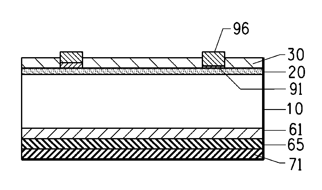
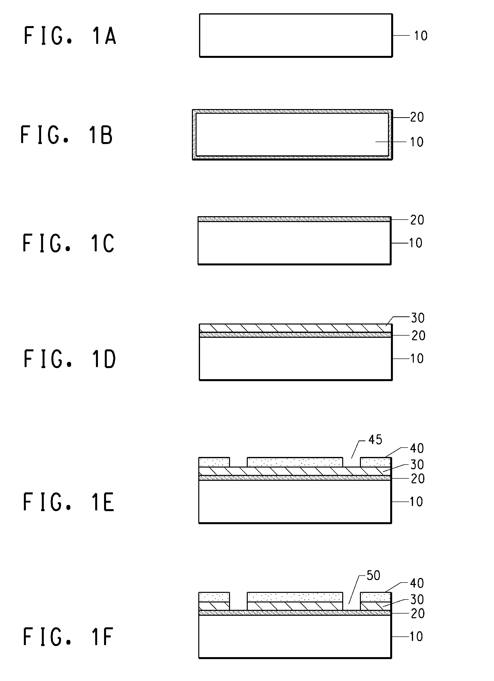
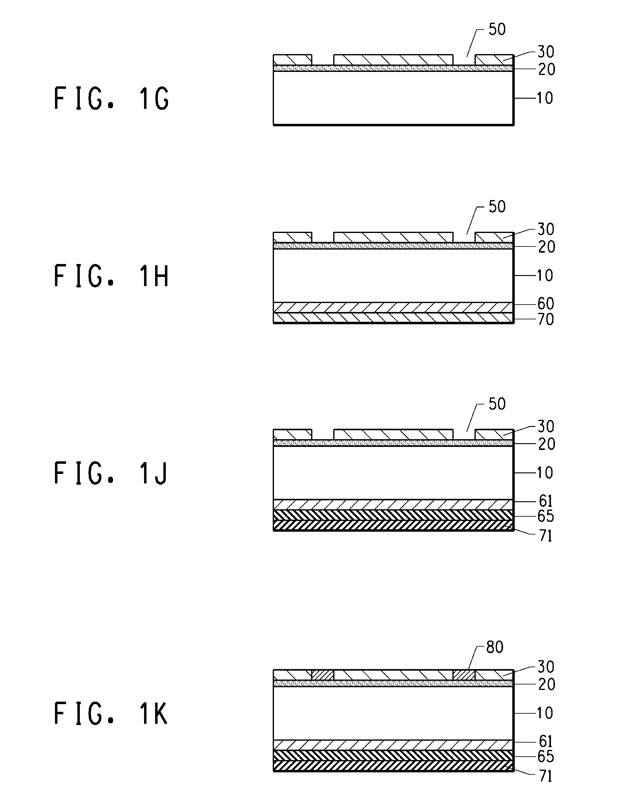
[0043]Photovoltaic devices having a low Shottky barrier height electrode contact to n-type silicon are disclosed. Also disclosed are methods for making photovoltaic devices having a low Shottky barrier height electrode contact to n-type silicon. The disclosed photovoltaic devices are solar cells but they may also be other photovoltaic devices having electrode contacts to n-type silicon such as photodetectors or light emitting diodes. The disclosed embodiment is a solar cell with a front face electrode on n-type silicon having a low Shottky barrier height electrode contact comprised of silicides comprising one or more transition metals or rare earth metals.

[0044]As used herein, the term “reactive metal” refers to a metal or mixtures of metals that reacts with silicon on firing to a form a stable highly conductive metal silicide. Such metals may include metals or mixtures thereof from titanium (Ti), zirconium (Zr), hafnium (Hf), tantalum (Ta), niobium (Nb) vanadium (V), chromium, (Cr)...


PUM

PropertyMeasurementUnit
diameteraaaaaaaaaa
weight percentaaaaaaaaaa

Abstract

Methods and compositions for making photovoltaic devices are provided. A metal that is reactive with silicon is placed in contact with the n-type silicon layer of a silicon substrate. The silicon substrate and reactive metal are fired to form a silicide contact to the n-type silicon layer. A conductive metal electrode is placed in contact with the silicide contact. A silicon solar cell made by such methods is also provided.

Description

FIELD OF THE INVENTION[0001]This invention is directed to photovoltaic devices, such as solar cells, light emitting diodes, and photodetectors. In particular, it is directed to compositions and processes for use in forming front face electrical contacts to the n-type silicon of a solar cell device.BACKGROUND OF THE INVENTION[0002]The present invention can be applied to a range of semiconductor devices, although it is especially effective in light-receiving elements such as photodetectors and solar cells. The background of the invention is described below with reference to solar cells as a specific example of the prior art.[0003]Conventional terrestrial solar cells are generally made of thin wafers of silicon (Si) in which a rectifying or p-n junction has been created and electrode contacts, that are electrically conductive, have been subsequently formed on both sides of the wafer. A solar cell structure with a p-type silicon base has a positive electrode contact on the base or backs...

Claims


Application Information

Patent Timeline
Patent Type & Authority Applications(United States)
IPC IPC(8): H01L31/07H01L31/00H01L31/0232H01L31/028H01B1/22
CPCH01B1/04Y02E10/50H01L31/022425Y02E10/547
Inventor BORLAND, WILLIAM J.MARIA, JON-PAUL
Owner EI DU PONT DE NEMOURS & CO
Why Eureka
Try Eureka