Phototransistor with source layer between barrier layer and photosensitive semiconductor layer and a gate layer for controlling the barrier height of the barrier layer

Inactive Publication Date: 2010-05-25
ST ERICSSON SA
View PDF1 Cites 2 Cited by
  • Summary
  • Abstract
  • Description
  • Claims
  • Application Information

AI Technical Summary

Benefits of technology

[0020]In use, the photocarriers created lower the barrier height markedly increasing the current through the gated transistor. The transistor accordingly has significant gain which allows for operation in low light levels.
[0024]In embodiments, the structure according to the invention makes use of the fact that holes have a higher effective mass than electrons and so are less able to tunnel though the barrier into the source layer than electrons. In this case, electrons can flow through the circuit from source to drain while holes accumulate at the barrier thereby effectively lowering the barrier height.
[0035](b) applying a frame gate voltage to the gate during a frame period, the frame gate voltage allowing any electrons created by illumination in the active region to pass the barrier but allow any holes created by illumination in the active region to accumulate in the photo-active layer at the barrier, thereby effectively reducing the effect of the barrier to electrons and increasing the electron current;

Problems solved by technology

Unfortunately it is difficult to make bipolar transistors with good performance in amorphous silicon or polysilicon which are suitable for so-called large area technologies, such as those used in imagers.
However, such prior art phototransistors are not very sensitive since no more than one electron and one hole is created per photon.
This means that high light levels are required.

Method used


Image

  • Phototransistor with source layer between barrier layer and photosensitive semiconductor layer and a gate layer for controlling the barrier height of the barrier layer
  • Phototransistor with source layer between barrier layer and photosensitive semiconductor layer and a gate layer for controlling the barrier height of the barrier layer
  • Phototransistor with source layer between barrier layer and photosensitive semiconductor layer and a gate layer for controlling the barrier height of the barrier layer

Examples


Embodiment Construction

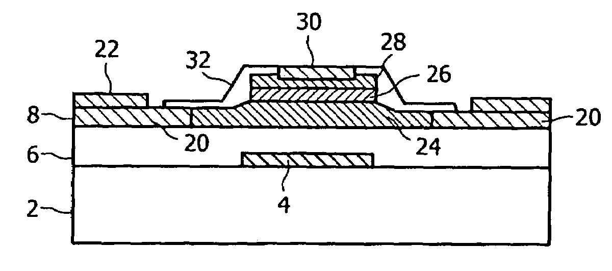
[0049]It should be noted that the Figures are schematic and not to scale. In particular, the thickness of the layers is in many cases exaggerated.

[0050]Referring to FIG. 2, a substrate 2 is provided, of glass or plastic. A gate layer 4 is formed over the substrate, and the whole surface covered in turn with a gate insulator layer 6 of Silicon Nitride. Above this is provided a layer of photosensitive semiconductor 8, which in this example comprises amorphous silicon (a-Si:H). A drain region 20 of the photosensitive semiconductor layer 8 is doped strongly n-type, and a drain contact 22 provided connecting to the drain region 20.

[0051]A thin barrier layer 26 of heavily doped p-type material is formed over an active region 24 of the photosensitive semiconductor layer 8, and a source layer 28 doped n-type is formed over the thin barrier layer 26. A transparent source electrode 30 is formed to connect to the source layer 28. In this example, the source electrode is of indium tin oxide.

[00...


PUM


Abstract

A photo transistor has an active region spaced from a source by barrier. A drain is laterally spaced from the active region. Light incident on the active region creates electron-hole pairs. Holes accumulate at the barrier and modulate the effective barrier height to electrons. A gate reset voltage then is applied to gate which lower the barrier allowing the holes to escape.

Description

BACKGROUND[0001]1. Technical Field[0002]The invention relates to a phototransistor and a method of operation of such a phototransistor.[0003]2. Description of the Related Art[0004]Phototransistors are useful for detecting optical information in general and low light levels in particular.[0005]A bipolar phototransistor is a classic example of a phototransistor that amplifies the photocurrent generated by incident light. The bipolar transistor has good output characteristics since the output is a high impedance current source which is easy to interface. Unfortunately it is difficult to make bipolar transistors with good performance in amorphous silicon or polysilicon which are suitable for so-called large area technologies, such as those used in imagers.[0006]Thin film phototransistors do exist and a conventional thin film phototransistor is illustrated in FIG. 1. The structure is formed on a substrate 2, typically glass or plastic. A gate 4 is formed over the substrate, and the whole...

Claims


Application Information

Patent Timeline
IPC IPC(8): H01L31/00H01L29/417H01L29/45H01L29/786H01L31/112H01L31/113
CPCH01L29/41733H01L31/1136H01L29/78678H01L29/458H01L31/112
Inventor SHANNON, JOHN M.BROTHERTON, STANLEY D.
Owner ST ERICSSON SA
Why Eureka
Try Eureka