

Metal-Gate High-K Reference Structure
a high-k reference structure and metal-gate technology, applied in the direction of semiconductor devices, electrical apparatus, transistors, etc., can solve the problems of limiting device scaling, increasing the effective gate dielectric layer thickness, and the depletion effect of the doped polysilicon gate conductor layer
- Summary
- Abstract
- Description
- Claims
- Application Information
AI Technical Summary
Benefits of technology
Problems solved by technology
Method used
Image

Examples
Embodiment Construction
[0023]The embodiments of the invention and the various features and advantageous details thereof are explained more fully with reference to the non-limiting embodiments that are illustrated in the accompanying drawings and detailed in the following description.
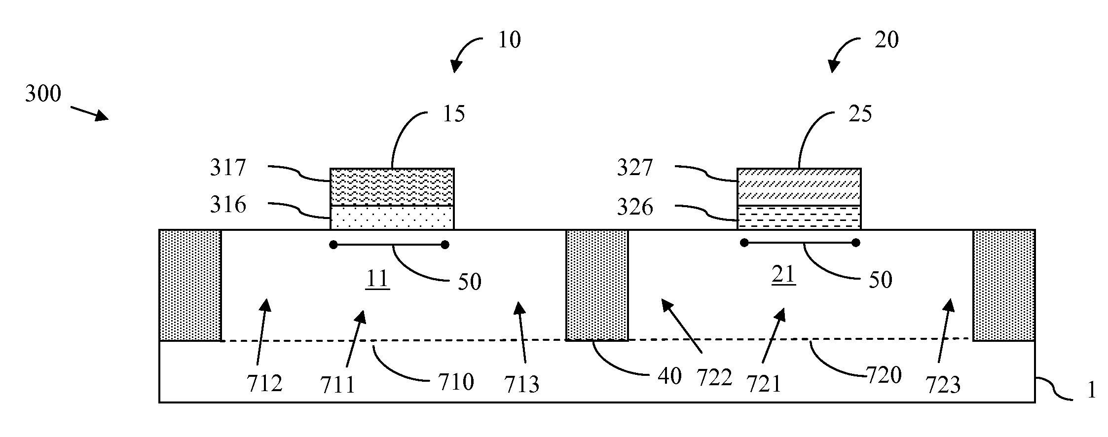
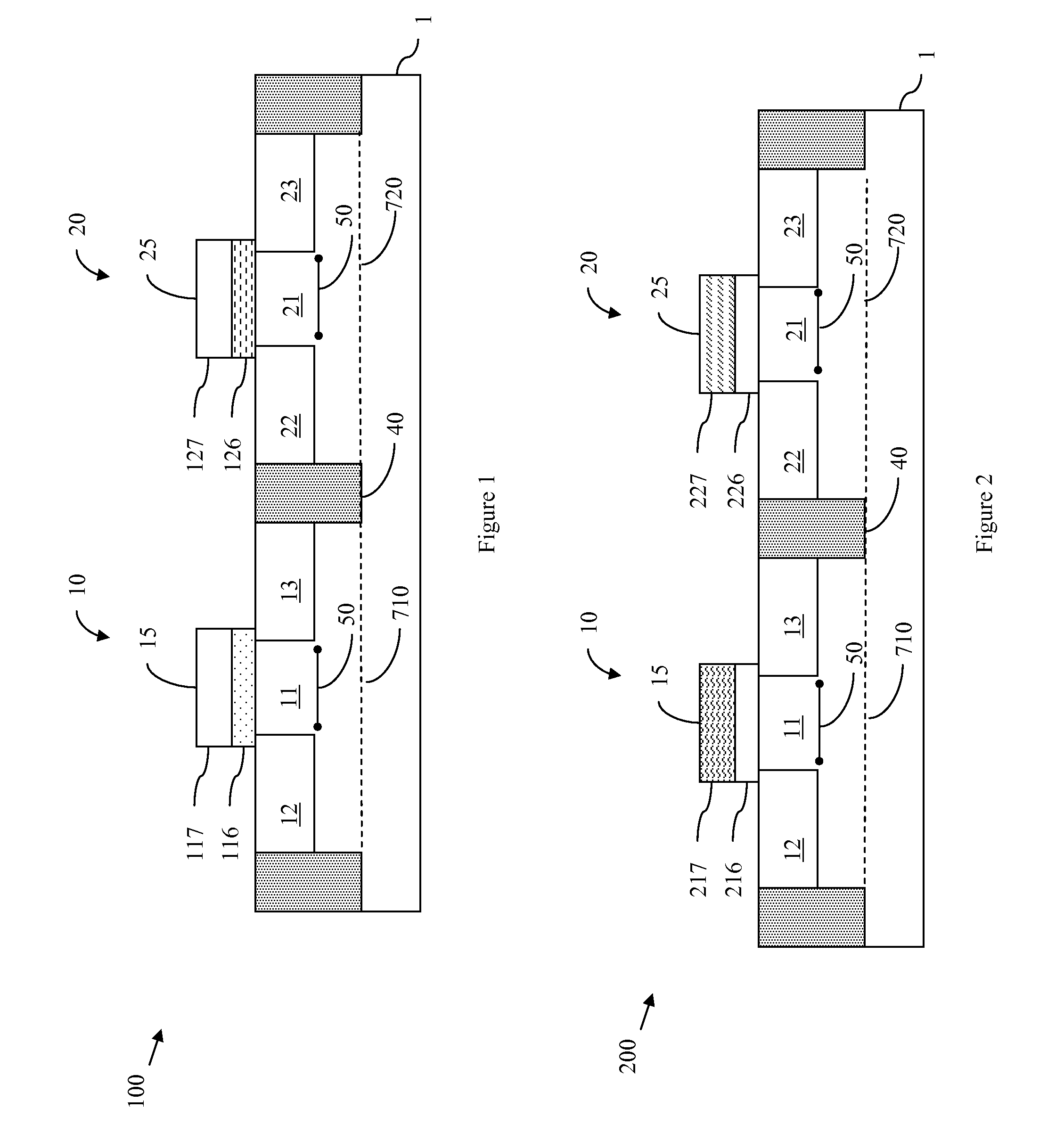
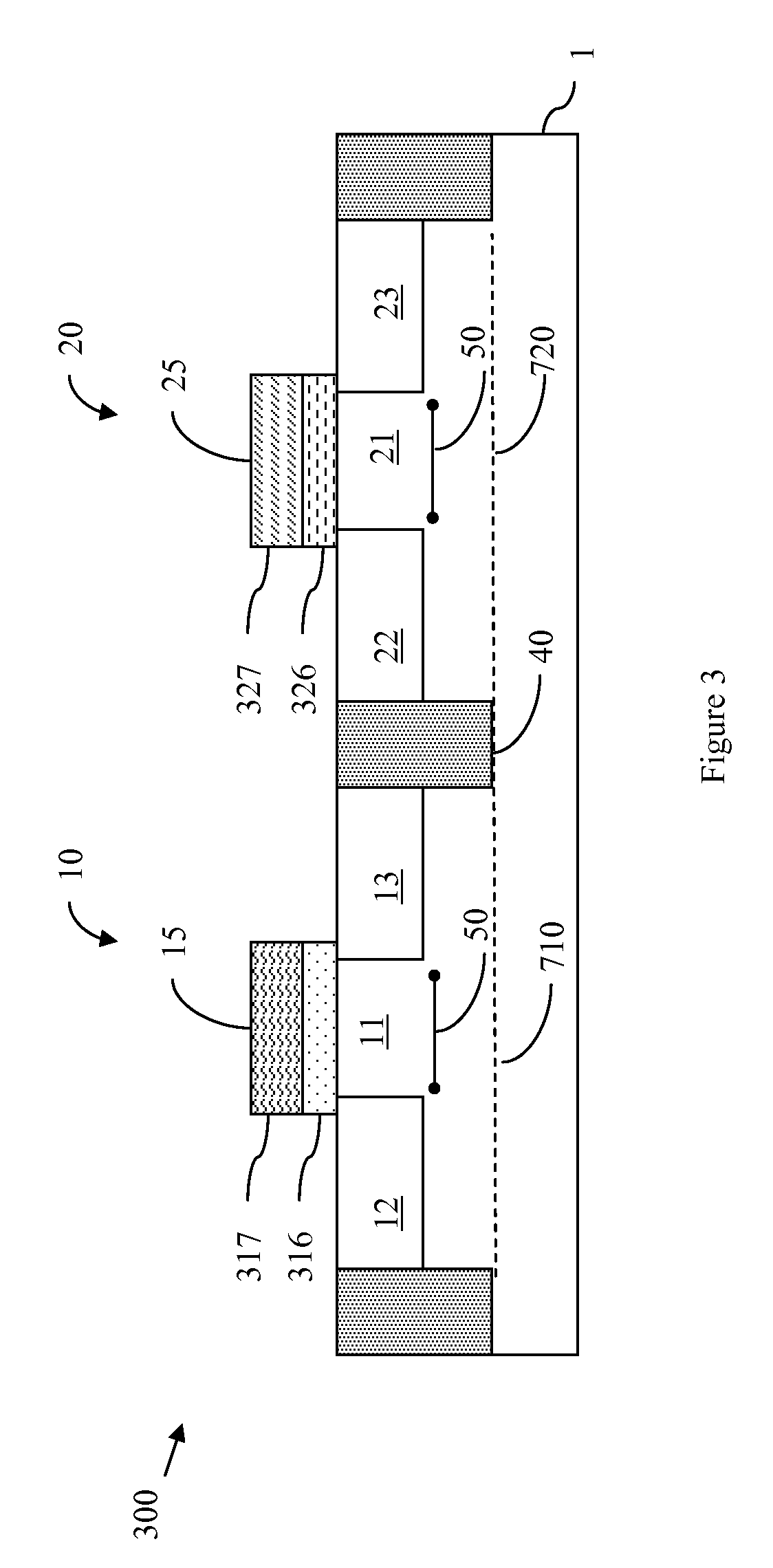
[0024]As mentioned above, in new technology generations, conventional gate stack structures are being replaced by high-k dielectric-metal gate stack structures. The ability to manipulate the effective work functions of such gate stacks, by varying the gate dielectric materials and / or the gate conductor materials, allows for the creation of improved analog functions. For example, disclosed herein are embodiments of an integrated circuit structure that takes advantage of such high-k dielectric-metal gate stacks. Specifically, the disclosed circuit structure embodiments incorporate at least two field effect transistors (FETs) that have the same conductivity type and also the same channel characteristics (i.e., same channel width ...
PUM
 Abstract
Description
Claims
Application Information