
Semiconductor device and power converter using the same

a technology of semiconductors and power converters, applied in semiconductor devices, power conversion systems, basic electric elements, etc., can solve the problems of backward overvoltage noise vp tending to be further increased, the voltage induced on the gate resistance cannot be sufficiently reduced, and the switch loss is largely influenced, so as to avoid the increase of conduction loss, reduce the loss of switching, and secure the effect of low noise characteristics

Active Publication Date: 2010-02-18
HITACHI POWER SEMICON DEVICE
View PDF4 Cites 25 Cited by
  • Summary
  • Abstract
  • Description
  • Claims
  • Application Information

AI Technical Summary

Benefits of technology

[0017]From the view of the above respects, it is an object of the present invention to provide a semiconductor device which can reduce a switch loss while avoiding increase of the conduction loss of an IGBT and securing a low noise characteristic, and also a power converter using the semiconductor device.
[0020]In accordance with the present invention, the IGBT can avoid increase of a conduction loss, secure a low noise characteristic and also reduce a switch loss. The power converter for use in an inverter system or the like using the semiconductor device can increase an efficiency.

Problems solved by technology

However, it has been found that the aforementioned IGBT of FIG. 13 has problems which follow.
Thus, even the gate resistance is made large to control the displacement current, the voltage induced on the gate resistance cannot be sufficiently reduced, and on the contrary, an increase in the turn-on time results in that the switch loss is largely influenced.
The backward overvoltage noise Vp tends to be further increased upon small-current turn-on operation.

Method used


Image

  • Semiconductor device and power converter using the same
  • Semiconductor device and power converter using the same
  • Semiconductor device and power converter using the same

Examples


embodiment 1

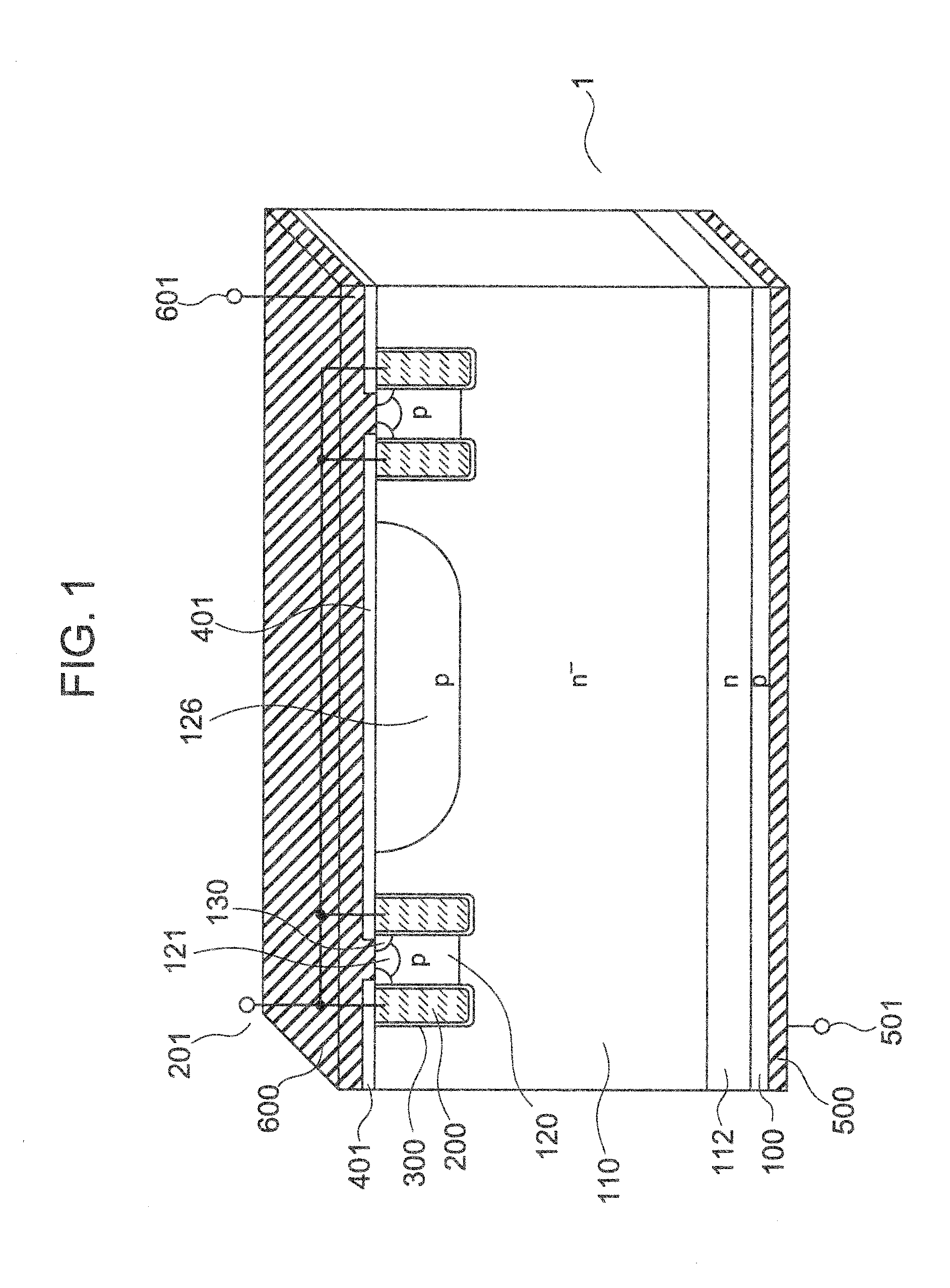
[0041]FIG. 1 shows a cross-sectional view of a semiconductor device in accordance with a first embodiment of the present invention. In FIG. 1, constituent elements having the same reference numerals or symbols are denoted by the same numerals or symbols as those in FIG. 13.

[0042]As shown in the same drawing, in the present embodiment, in place of a floating p layer 125 adjacent to a gate electrode 200 in the structure of a prior art of FIG. 13, a floating p layer 126 is provided between trench gates with a drift n− layer 110 disposed therebetween.

[0043]FIG. 1 is featured in that the floating p layer 126 is spaced from the trench gates by a distance with the drift n− layer 110 disposed therebetween. With such a structure, the drift n− layer 110 is exposed to its main surface to the drift n− layer 110 and to the trench gates at the spaced zones.

[0044]Even in FIG. 1, similar to FIG. 13, the floating p layer 126 has such a state as to have a potential transiently higher than the trench ...

embodiment

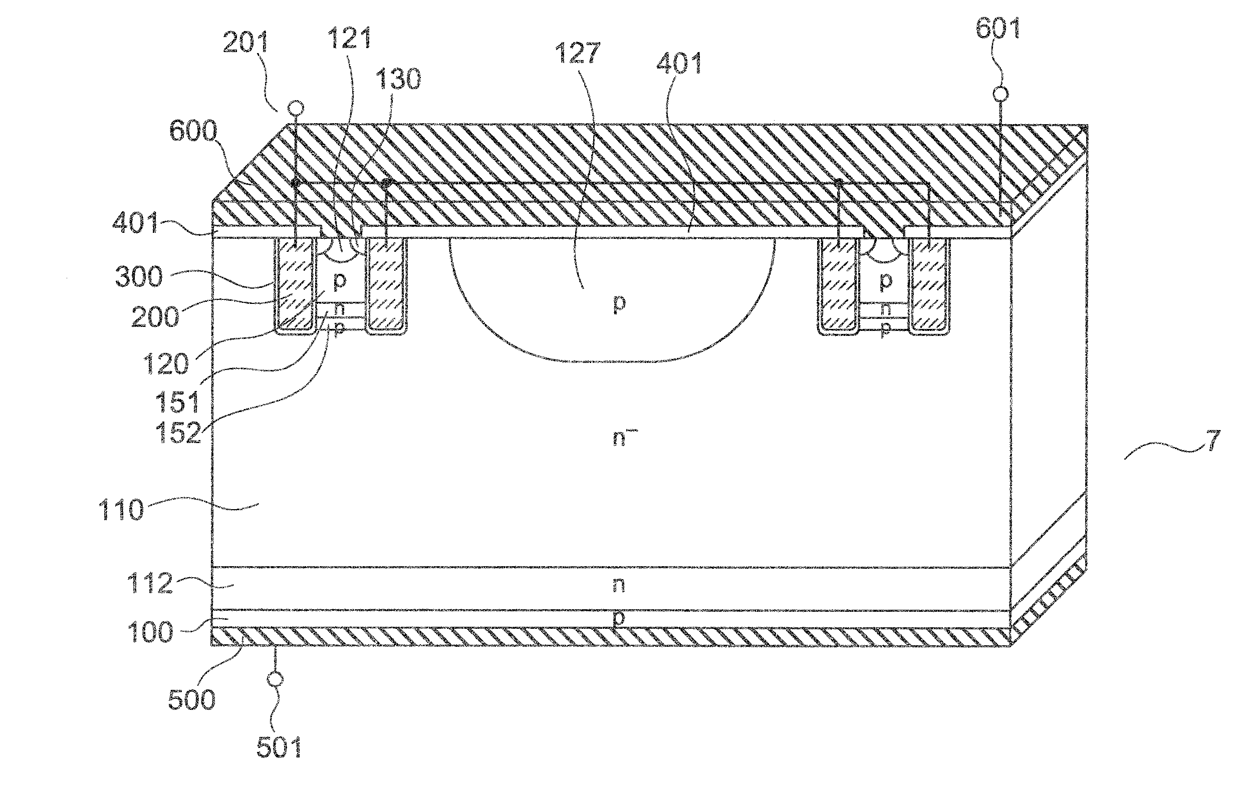
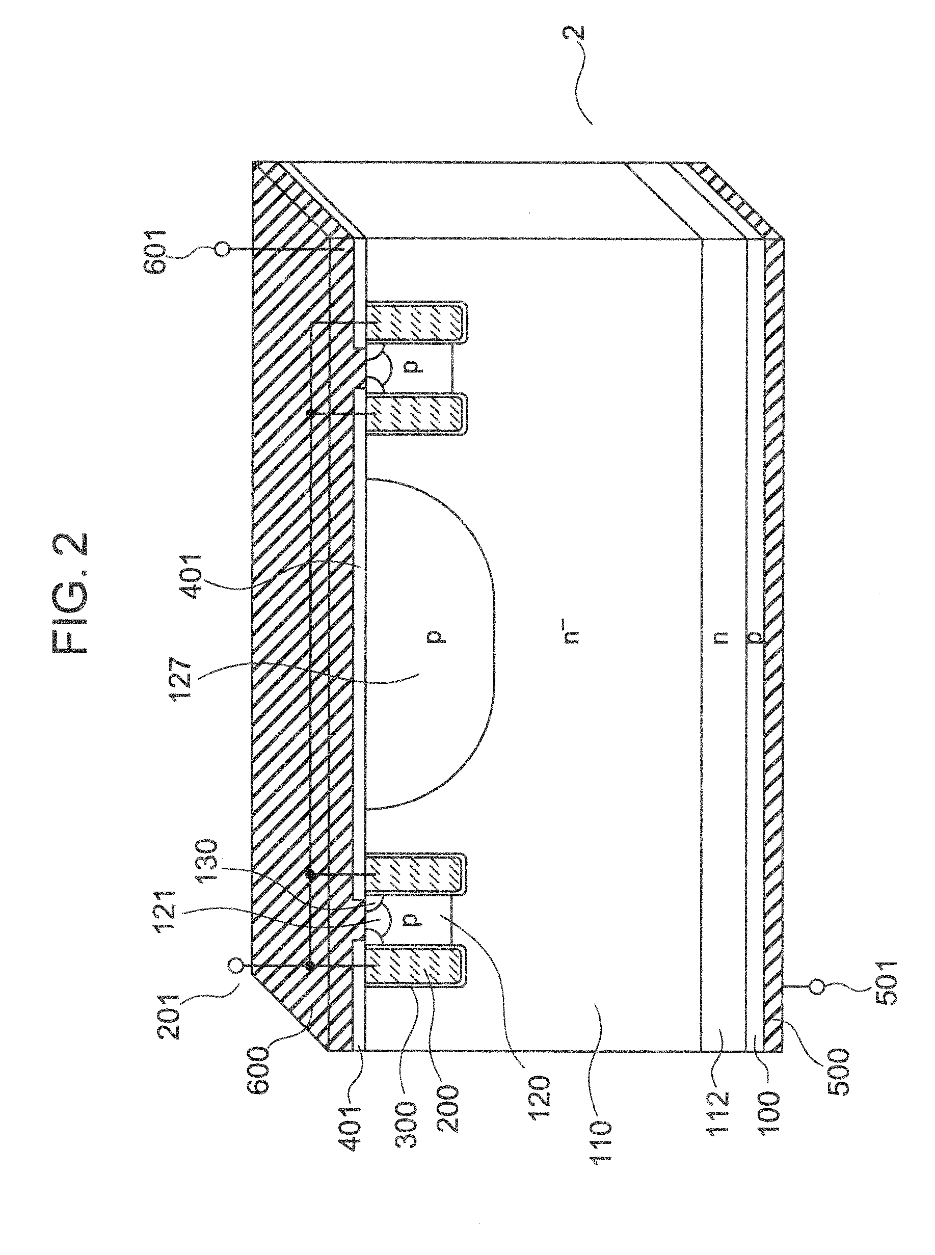
[0057]FIG. 2 shows a cross-sectional view of a structure in accordance with a second embodiment of the present invention. In FIG. 2, constituent elements having the same reference numerals or symbols as those in FIG. 1 are denoted by the same reference numerals or symbols. In FIG. 2, reference numeral 127 denotes a floating p layer.

[0058]FIG. 2 is featured in that the floating p layer 126 illustrated in FIG. 1 is replaced with the floating p layer 127 of a structure wherein the floating p layer is formed to be deeper than the channel p layer 120 and the trench MOS gates, thus increasing a breakdown voltage.

[0059]With the structure of FIG. 2, it can be expected to further increase the breakdown voltage while keeping the effects of FIG. 1. In an OFF state, depletion is advanced from an interface between the channel p layer 120 and the drift n− layer 110, and equipotential lines expanded parallelly to the interface reach interior of the drift n− layer 110 located between the gates and ...

embodiment 3

[0062]FIGS. 3, 4 and 5 show cross-sectional views of a structure in accordance with a third embodiment of the present invention. In FIGS. 3, 4 and 5, constituent elements having the same reference numerals or symbols as those in FIG. 1 are denoted by the same reference numerals or symbols. Reference numeral 122 in FIG. 3 denotes a channel p layer, Reference numeral 123 in FIG. 4 denotes a channel p layer, and Reference numeral 124 in FIG. 5 denotes a channel p layer.

[0063]FIGS. 3, 4 and 5 are featured in that the channel p layers 122, 123 and 124 are made deeper than the channel p layer 120 in FIG. 1. More specifically, FIGS. 3, 4 and 5 are featured in a structure wherein the channel p layer has nearly the same depth as the trench MOS gates, a structure wherein the channel p layer has such a depth as to cover the lower side of the trench MOS gates, and a structure wherein the channel p layer has such a depth as to cover the trench MOS gates as far as the side surface thereof opposed...


PUM


Abstract

A semiconductor device which can avoid increase of a conduction loss of an IGBT, secure a low noise characteristic and also reduce a switch loss. The switching device is of a trench gate type, in which a drift n− layer 110 is exposed to its main surface to a floating p layer 126 and to trench gates. In other words, the floating p layer 126 is provided within the drift n− layer 110 to be spaced from the trench gates.

Description

BACKGROUND OF THE INVENTION[0001]The present invention relates to semiconductor devices and power converters using the semiconductor devices and more particularly, to a semiconductor device and a power converter using the semiconductor device, which are suitably used in wide applications ranging from small power equipment such as an air conditioner or a microwave oven to a large power equipment such as an inverter for use in railroad or ironworks.[0002]An insulated gate bipolar transistor (which will be referred to as IGBT, hereinafter) is a switching element which controls a current flowing between collector and emitter electrodes caused by a voltage applied to a gate electrode. A power range controllable by the switching element is between tens of watts and a level exceeding one hundred thousand watts, and a switching frequency range is also wide and between tens of hertz to hundreds of hertz. In order to make the most of such a feature, the IGBT is used in a broad fields ranging ...

Claims


Application Information

Patent Timeline
Patent Type & Authority Applications(United States)
IPC IPC(8): H02M7/537H01L27/06
CPCH01L29/0839H01L29/7397H01L29/1095
Inventor ARAI, TAIGAMORI, MATSUHIRO
Owner HITACHI POWER SEMICON DEVICE
Learn More