Electrostatic discharge protection device

Inactive Publication Date: 2010-02-25
UNITED MICROELECTRONICS CORP
View PDF6 Cites 17 Cited by
  • Summary
  • Abstract
  • Description
  • Claims
  • Application Information

AI Technical Summary

Benefits of technology

[0013]It is an advantage of the present invention ESD protection device that the claimed ESD protection device includes the first and second SCR elements disposed in the space where the double guard-rings are used to be disposed according to the conventional ESD protection device. Therefore, the dimension of the claimed invention ESD protection device does no

Problems solved by technology

The ESD phenomenon occurs when excess charges are transmitted from the input/output (I/O) pin to the integrated circuit too quickly, which damages the internal circuit.
However, the turned-on voltages of the parasitic bipolar transistors are high, and the gate oxide layer of an NMOS or PMOS transistor is becoming thinner with the continuing scaling-down of semiconductor integrated circuit (IC) device dimensions, thus

Method used


Image

  • Electrostatic discharge protection device
  • Electrostatic discharge protection device
  • Electrostatic discharge protection device

Examples


first embodiment

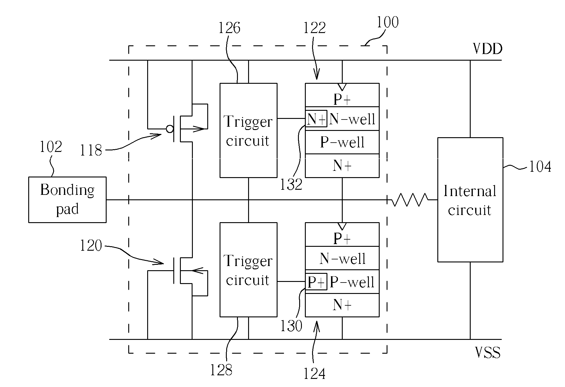
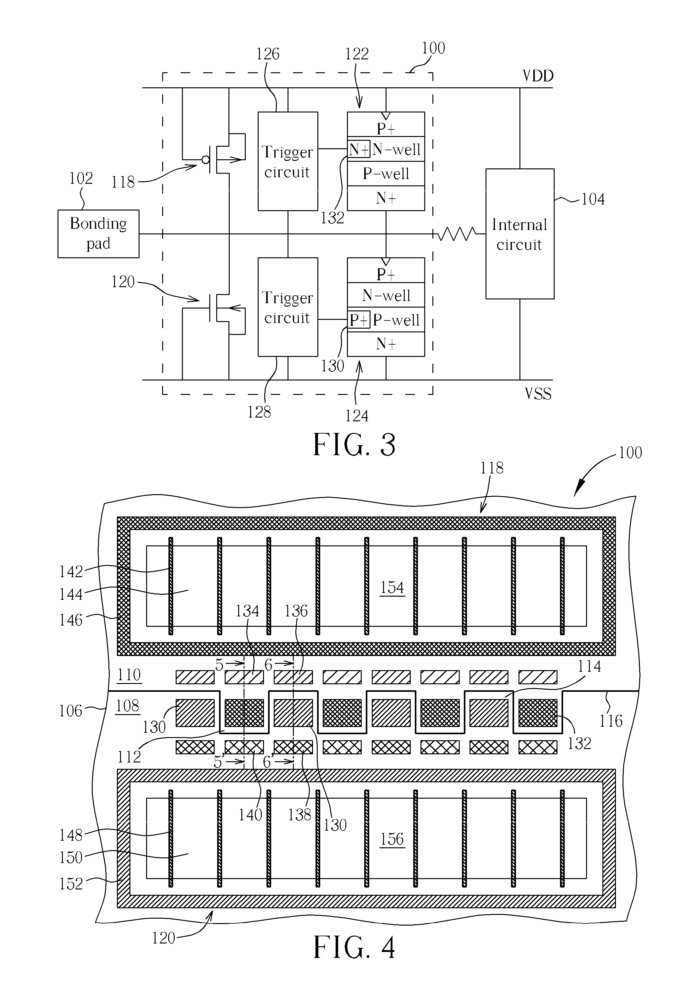
[0027]With reference to FIG. 3 and FIG. 4, FIG. 3 is an equivalent circuit diagram of an ESD protection device according to the present invention, and FIG. 4 is a top-view schematic diagram of the ESD protection device shown in FIG. 3. The present invention ESD protection device 100 is electrically connected to a bonding pad 102 (such as an I / O pin) and an internal circuit 104, comprising a PMOS transistor 118, an NMOS transistor 120, a first SCR element 122, and a second SCR element 124. The source of the PMOS transistor 118 and the drain of the NMOS transistor 120 are electrically connected to the internal circuit 104 and the bonding pad 102 respectively, and the drain of the PMOS transistor 118 and the anode of the first SCR element 122 are electrically connected to a first power terminal VDD, which may be a power supply terminal. The source of the NMOS transistor 120 and the cathode of the second SCR element 124 are electrically connected to the second power terminal VSS, which ...

second embodiment

[0033]FIG. 7 is a top-view schematic diagram of an ESD protection device 200 according to the present invention. The present invention ESD protection device 200 is disposed on a substrate 202, such as a P-type silicon substrate, and electrically connected to a bonding pad 102 and an internal circuit 104 as shown in FIG. 3. The ESD protection device 200 comprises a P-well 204 and an N-well 206 contiguously disposed on the surface of a substrate 202, wherein the P-well 202 and the N-well 204 respectively have a plurality of first protrudent portions 208 and a plurality of second protrudent portions 210, interlacedly arranged at a boundary 212 of the P-well 204 and N-well 206. The ESD protection device 200 further comprises a PMOS transistor 214 disposed in the N-well 206, an NMOS transistor 216 disposed in the P-well 204, a plurality of first P+ diffusion regions 218 disposed in each second protrudent portions 210 respectively, a plurality of first N+ diffusion regions 220 disposed in...

fifth embodiment

[0038]With reference to FIG. 11, FIG. 11 is a top-view schematic diagram of an ESD protection device 300 according to the present invention. Similarly, the present invention ESD protection device 300 is electrically connected to a bonding pad 102 and an internal circuit 104 as shown in FIG. 3, and is disposed on a surface of a substrate 302. The ESD protection device 300 comprises a P-well 304 and an N-well 306 contiguously arranged on the surface of the substrate 302. The P-well 304 and the N-well 306 has a boundary 316. The substrate 302 may be a P-type silicon substrate, and the P-well 304 may be considered as a portion of the P-type silicon substrate. The ESD protection device 300 further comprises a PMOS transistor 308 disposed in the N-well 306, an NMOS transistor 310 disposed in the P-well 304, a plurality of first P+ diffusion regions 312, a plurality of second P+ diffusion regions 314, a plurality of first N+ diffusion regions 318 and a plurality of second N+ diffusion regi...


PUM


Abstract

An ESD protection device includes a p-well with first protrudent portions, an N-well with second protrudent portions, a P-well/N-well boundary, a PMOS transistor disposed in the N-well, an NMOS transistor disposed in the P-well, first P+ diffusion regions in the first protrudent portions, first N+ diffusion regions in the second protrudent portions, second P+ diffusion regions disposed between the PMOS transistor and the second protrudent portions, second N+ diffusion regions disposed between the NMOS transistor and the first protrudent portions, third P+ diffusion regions disposed between the NMOS transistor, the boundary, and two adjacent second P+ diffusion regions, and third N+ diffusion regions disposed between the PMOS transistor, the boundary, and two adjacent second N+ diffusion regions, wherein the first and second protrudent portions are interlacedly arranged at the boundary.

Description

BACKGROUND OF THE INVENTION[0001]1. Field of the Invention[0002]The present invention relates to an electrostatic discharge (ESD) protection device, and more particularly, to an ESD protection device having a P-type metal-oxide semiconductor (PMOS) transistor, an N-type metal-oxide semiconductor (NMOS) transistor, and two parasitic silicon controlled rectifier (SCR) elements.[0003]2. Description of the Prior Art[0004]ESD usually occurs in semiconductor devices. The ESD phenomenon occurs when excess charges are transmitted from the input / output (I / O) pin to the integrated circuit too quickly, which damages the internal circuit. In order to solve such a problem, manufacturers normally build an ESD protection device between the internal circuit and the I / O pin. The ESD protection device is initiated before the pulse of ESD enters the internal circuit for discharging the excess charges, and thus ESD-related damage is decreased.[0005]Referring to FIG. 1, FIG. 1 is an equivalent circuit d...

Claims


Application Information

Patent Timeline
IPC IPC(8): H01L23/62
CPCH01L27/0262
Inventor LIN, TA-CHENGWU, TE-CHANGSUN, YU-MINGLIN, MAUNG-WAI
Owner UNITED MICROELECTRONICS CORP
Why Eureka
Try Eureka