3D integrated circuit device fabrication with precisely controllable substrate removal

a technology of integrated circuit devices and fabrication techniques, applied in semiconductor devices, instruments, computing, etc., can solve the problems of general purpose substrate thinning techniques that do not allow the production of final substrates, and only work for silicon-on-insulator (soi) wafers, and achieve the effect of not working for soi circuits having structures

Active Publication Date: 2010-02-25
TAIWAN SEMICON MFG CO LTD
View PDF17 Cites 25 Cited by
  • Summary
  • Abstract
  • Description
  • Claims
  • Application Information

AI Technical Summary

Problems solved by technology

One problem experienced in the fabrication of 3D integrated circuit devices is that general purpose substrate thinning techniques do not allow the final substrate to be produced with a controlled thickness that is thin enough to allow high-density through-silicon vias with reasonable aspect ratios to be realized.
However, this technique only works for silicon-on-insulator (SOI) wafers.
Further, even with an SOI wafer, this technique does not work for SOI circuits having structures that extend below the buried oxide, such as an embedded DRAM (e-DRAM) trench.
However, this technique greatly increases the manufacturing cost.
Such protection is required because, while the SOI wafer acts as an etch stop, it does not provide selectivity between the different substrates.
However, this technique does not allow the wafers to be thinned aggressively and creates uniformity problems.
Further, for integrated circuits that require a high density of 3D vias, this technique also forces the use of high aspect ratio vias that cannot be filled with copper.
Another problem experienced in the fabrication of 3D integrated circuit devices is that stacking three or more layers to create a multi-layer stack leads to yield loss.
However, the use of such a temporary handle wafer (e.g., a glass wafer) induces overlay distortions that degrade the alignment overlay between the wafers.
That is, this technique does not allow high-precision optical alignment in subsequent lithographic steps.
However, such direct face-to-face joining is problematic because the bottom wafer (which usually is a logic wafer) must then be used as the handle wafer throughout the stacking process.
This increases the probability of catastrophic failure and loss of the entire integrated circuit, including the logic wafer that is often the most expensive wafer in the stack.

Method used


Image

  • 3D integrated circuit device fabrication with precisely controllable substrate removal
  • 3D integrated circuit device fabrication with precisely controllable substrate removal
  • 3D integrated circuit device fabrication with precisely controllable substrate removal

Examples


Embodiment Construction

[0016]Preferred embodiments of the present invention will be described in detail hereinbelow with reference to the attached drawings.

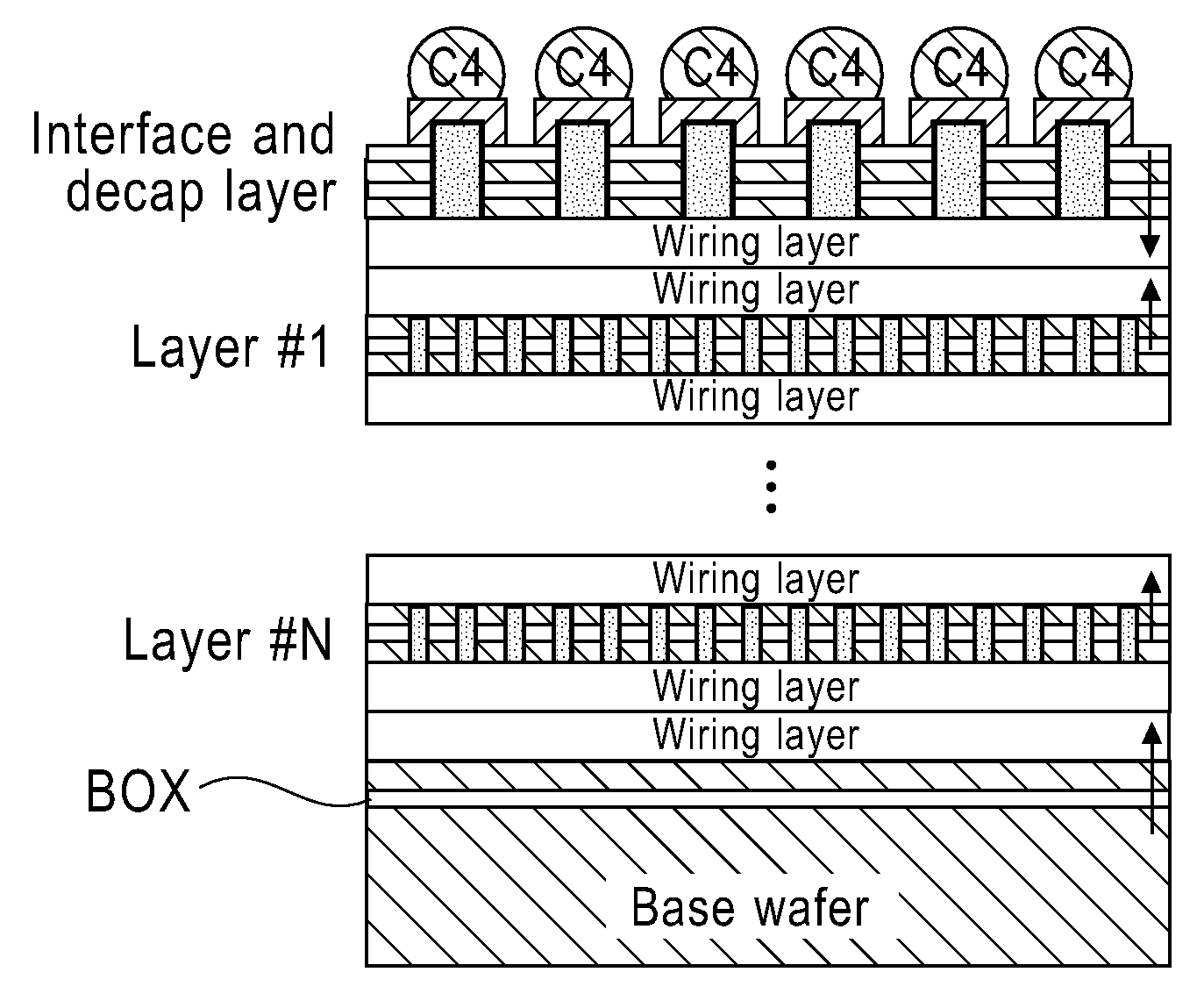
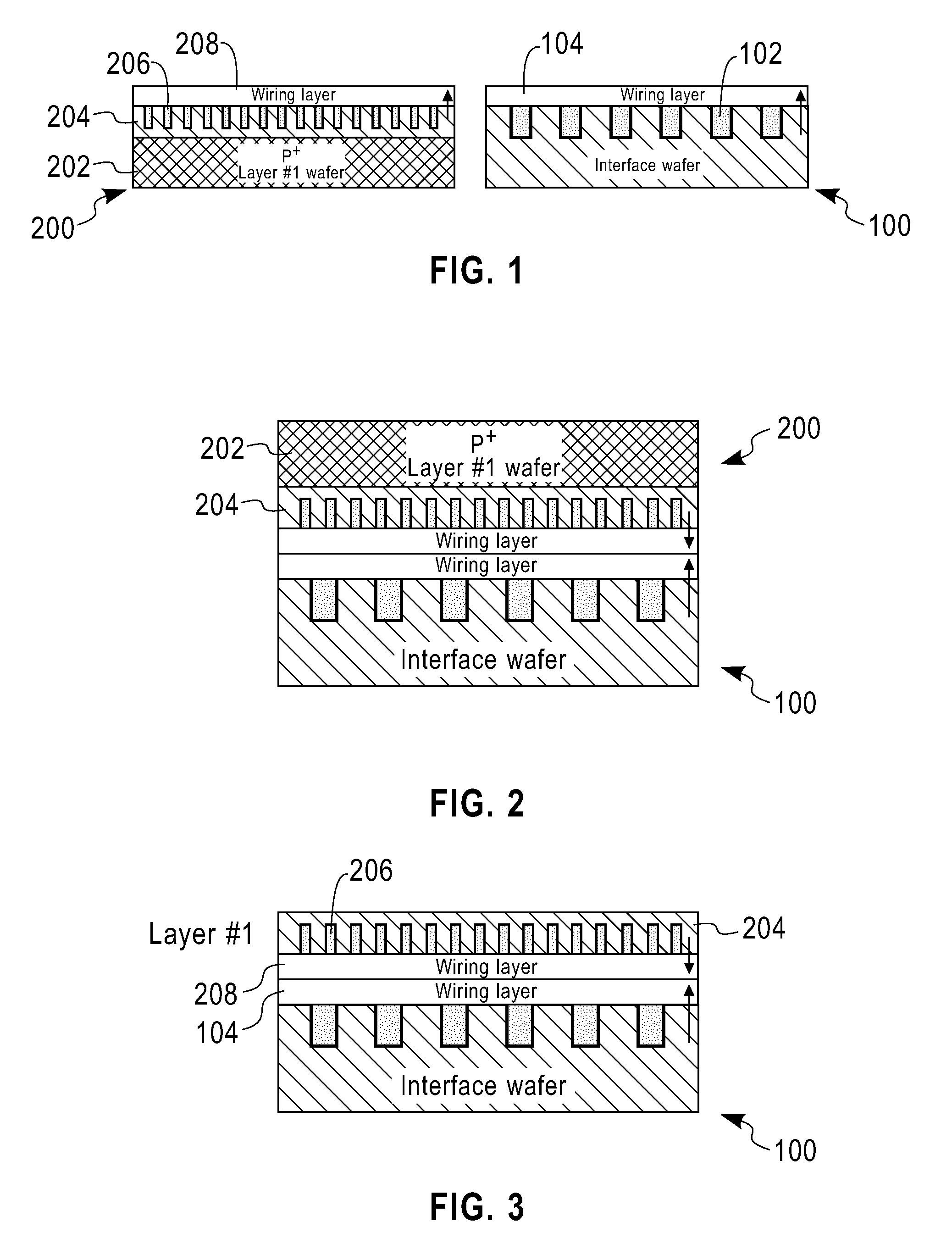
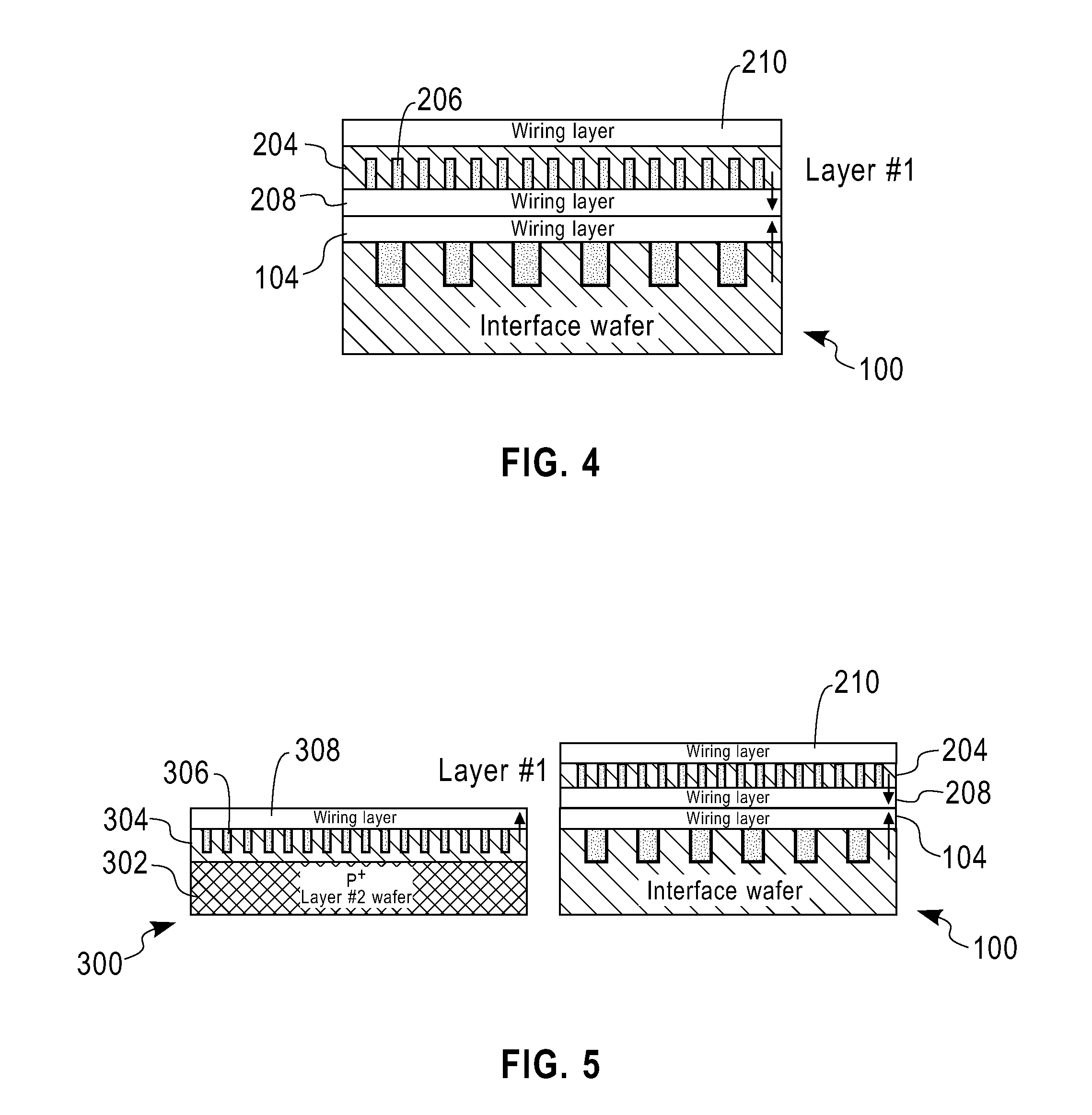
[0017]Embodiments of the present invention allow precisely controllable substrate removal during three-dimensional (3D) integrated circuit device fabrication by utilizing a P+ / P− substrate. The P+ / P− substrate is a P+ wafer that has a P− top active layer. In one exemplary embodiment, the P− top active layer is grown epitaxially on a P+ wafer and has a thickness of between about 5 and 20 microns. The P+ wafer and P− top active layer of the P+ / P− substrate allow controllable substrate removal down to very thin layers. Thus, the present invention overcomes the problem of a lack of controllable substrate thinning that is present in the known and previously proposed substrate thinning techniques for 3D integrated circuits. The controllability of substrate removal in the present invention allows low aspect ratio vias that can be filled with copper, so as to ...


PUM


Abstract

A method is provided for fabricating a 3D integrated circuit structure. According to the method, a first active circuitry layer wafer is provided. The first active circuitry layer wafer comprises a P+ portion covered by a P− layer, and the P− layer includes active circuitry. The first active circuitry layer wafer is bonded face down to an interface wafer that includes a first wiring layer, and then the P+ portion of the first active circuitry layer wafer is selectively removed with respect to the P− layer of the first active circuitry layer wafer. Next, a wiring layer is fabricated on the backside of the P− layer. Also provided are a tangible computer readable medium encoded with a program for fabricating a 3D integrated circuit structure, and a 3D integrated circuit structure.

Description

CROSS REFERENCE TO RELATED APPLICATIONS[0001]This application is related to application “3D Integrated Circuit Device Fabrication Using Interface Wafer As Permanent Carrier,” Ser. No. ______, now ______, and application “3D Integrated Circuit Device Having Lower-Cost Active Circuitry Layers Stacked Before Higher-Cost Active Circuitry Layer,” Ser. No. ______, now ______, which were filed on the same day as the present application and commonly assigned therewith to International Business Machines Corporation. These related applications are incorporated herein by reference in their entirety.FIELD OF THE INVENTION[0002]The present invention generally relates to the field of integrated circuits, and more particularly relates to the fabrication of three-dimensional (3D) integrated circuit devices.BACKGROUND OF THE INVENTION[0003]Three-dimensional (3D) integrated circuit devices are experiencing extremely active development in the industry. One problem experienced in the fabrication of 3D ...

Claims


Application Information

Patent Timeline
Patent Type & Authority Applications(United States)
IPC IPC(8): H01L21/50H01L21/67H01L27/12
CPCH01L27/0688H01L24/11H01L27/105H01L2924/14H01L2224/05024H01L2224/05008H01L2224/05009H01L2224/0557H01L2224/05568H01L2224/05147H01L2224/05184H01L2924/00014H01L24/05H01L2924/00H01L2224/05599H01L25/065H01L21/70
Inventor FAROOQ, MUKTA G.HANNON, ROBERTIYER, SUBRAMANIAN S.KOESTER, STEVEN J.PURUSHOTHAMAN, SAMPATHYU, ROY R.
Owner TAIWAN SEMICON MFG CO LTD
Why Eureka
Try Eureka