Noncontact IC tag label and method of manufacturing the same

Active Publication Date: 2010-03-04
DAI NIPPON PRINTING CO LTD
View PDF6 Cites 70 Cited by
  • Summary
  • Abstract
  • Description
  • Claims
  • Application Information

AI Technical Summary

Benefits of technology

[0023](1) According to the noncontact IC tag label of the present invention, materials costs can be reduced since the label does not use the antenna-supporting base film that has been a mandatory structural material of a conventional noncontact IC tag label.
[0024](2) In the noncontact IC tag label manufacturing method of the present invention, manufacturing costs can be reduced since the label can be completed by die cutting with an antenna-cutting die, without using a conventional etching method.
[0025](3) In addition, in the noncontact IC tag label manufacturing method of the present inventio

Problems solved by technology

Conventional noncontact IC tag labels have had the problem that their structure absolutely requiring the use of the base film for supporting the antenna from the underside increases the cost of the data carrier.
Also, conventional manufacturing methods have had the problem that in addition to the use of resist-forming process equipment and etching equipment for resist printing and photomasking, etching requires post-processing and the preparatio

Method used


Image

  • Noncontact IC tag label and method of manufacturing the same
  • Noncontact IC tag label and method of manufacturing the same
  • Noncontact IC tag label and method of manufacturing the same

Examples


first example

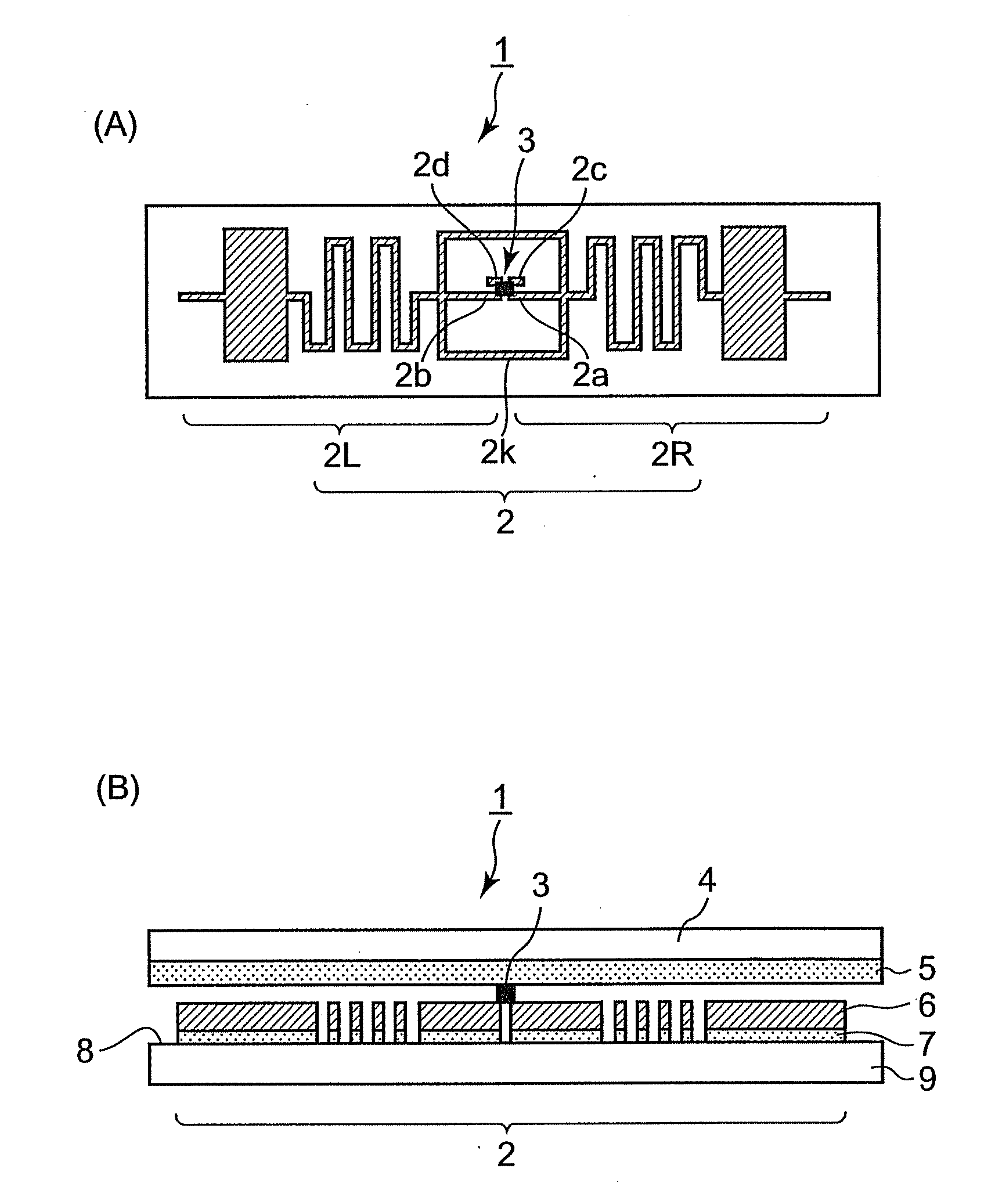
[0082]An aluminum foil having 120 mm wide by 15 μm thick, coated with a polyester-based hot-melting adhesive agent (thermo adhesive resin layer 7h) to a thickness of 20 μm, is used as a continuum of an antenna material 2m. Kraft paper surface-coated with silicone to a width of 120 mm and a thickness of 100 μm is used as a release paper 9. The antenna material 2m is overlaid upon the release paper 9 so as to face upward, and then supplied to a test-produced flat-bed antenna-cutting die 20 containing a heat source. A dipole antenna 2 of the shape as shown in FIG. 1 is continuously die-cut at 50-mm intervals. The cutting die 20 is a device having the foregoing air holes 81 and constructed to connect to a suction / discharge device 82. The heat source is also inserted within a receiving die side of the cutting die so that the thermo adhesive resin layer 7h is fully heated and fused.

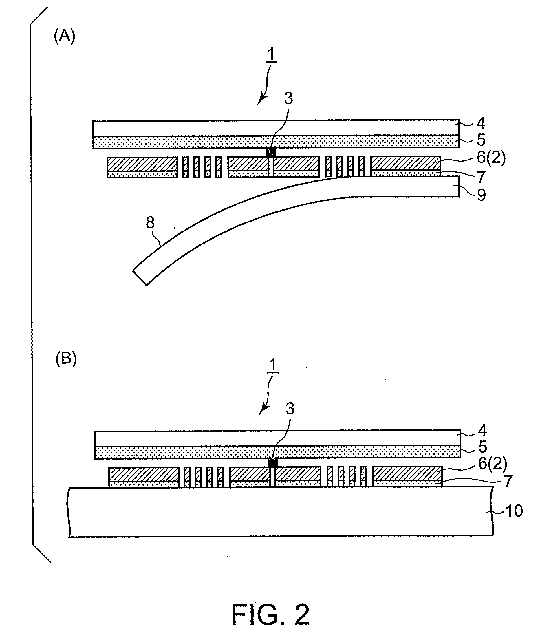
[0083]After a portion of the continuum 10w of the die-cut antenna material 2m is moved past between separati...

second example

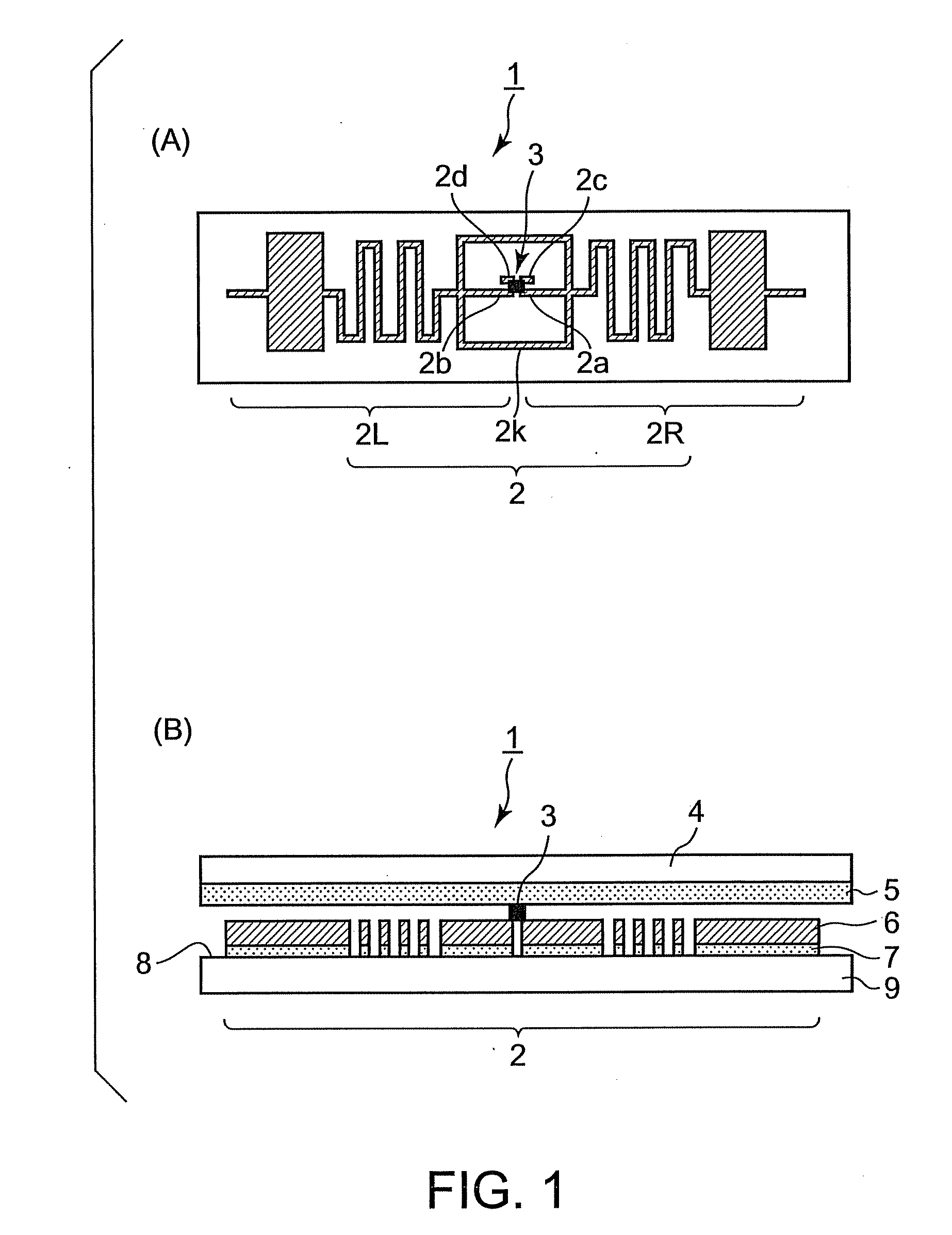
[0084]An aluminum foil having 120 mm wide by 15 μm thick, including an adhesive resin layer 7 coated with an acrylic pressure-sensitive adhesive agent 7n to a thickness of 25 μm, is used as a continuum of an antenna material 2m. Kraft paper surface-coated with silicone to a width of 120 mm and a thickness of 80 μm is used as a release paper 9. The antenna material 2m is overlaid upon the release paper 9 so as to face upward, and then supplied to the flat-bed antenna-cutting die 20 used in the first example. However, the present (second) example does not use a heat source.

[0085]A dipole antenna 2 of the shape as shown in FIG. 1 is continuously die-cut at 50-mm intervals. After a portion of the continuum 10w of the die-cut antenna material 2m is moved past between separating rollers 20a and 20b, then a necessary section of the antenna 2 is separated from an unnecessary section, and a precise antenna pattern shape is obtained in a thermally transferred condition on the surface of the r...


PUM


Abstract

This invention provides a thin type of noncontact IC tag label that allows materials costs to be reduced without using an antenna-supporting base film. The noncontact IC tag label includes an electroconductive layer 6 of a required antenna pattern shape, an IC chip 3 mounted on one face of the electroconductive layer 6, and a surface protection sheet 4 supporting the electroconductive layer 6 and the IC chip 3 from a side of the one face of the electroconductive layer 6 via a first pressure-sensitive adhesive layer 5. An adhesive resin layer 7 having the same shape as the antenna pattern shape of the electroconductive layer 6 is provided on the other face of the electroconductive layer 6. The adhesive resin layer 7 is temporarily bonded in separable manner onto a release paper 9 formed from paper or a plastic base material.

Description

CROSS-REFERENCE TO RELATED APPLICATIONS[0001]The present patent application benefits from Japanese application serial number JP2006-297252, filed on Nov. 1, 2006. The entire disclosure of this earlier application is hereby incorporated by reference in this application.TECHNICAL FIELD[0002]The present invention relates generally to noncontact IC tag labels and methods of manufacturing the same. More particularly, the invention concerns a noncontact IC tag label constructed without a base material, unlike conventional noncontact IC tag labels, and including an antenna pattern supported by a surface protection sheet. In addition, the invention is directed to a method of manufacturing the above noncontact IC tag label.BACKGROUND ART[0003]Noncontact IC tag labels are a medium that is also termed a radio-frequency identification (RFID) tag or a noncontact data carrier. This type of medium has an IC chip retaining the information allowing the identification of a specific commodity / product,...

Claims


Application Information

Patent Timeline
IPC IPC(8): G06K19/07H01L21/607
CPCG06K19/07722G06K19/07749G06K19/0775H01Q1/2225H01L2924/0002H01L2924/00
Inventor OGATA, TETSUJISAKATA, HIDETO
Owner DAI NIPPON PRINTING CO LTD
Why Eureka
Try Eureka