Sheet Member for Improving Communication, and Antenna Device and Electronic Information Transmitting Apparatus Provided Therewith

a technology of electronic information and transmission apparatus, which is applied in the direction of electrically short antennas, antenna details, antennas, etc., can solve the problems of significant attenuation of electromagnetic wave signals, inability of tag b>1/b> to perform wireless communication, etc., to achieve the effect of improving communication

Inactive Publication Date: 2010-03-04
NITTA CORP
View PDF12 Cites 66 Cited by
  • Summary
  • Abstract
  • Description
  • Claims
  • Application Information

AI Technical Summary

Benefits of technology

[0012]It is an object of the invention to provide, instead of a radio wave absorbing member that attenuates electromagnetic energy, a sheet member for improving communication, capable of storing communication energy and enabling wireless communication to be suitably performed in the vicinity of a communication jamming member, and an antenna device and an electronic information transmitting apparatus provided therewith.

Problems solved by technology

When the energy is absorbed in this manner, electromagnetic wave signals are significantly attenuated, which makes it impossible for the tag 1 to perform wireless communication.
This phenomenon also makes it impossible for the tag 1 to perform wireless communication.
In a case where a conductive material is present in the vicinity of an antenna element, the input impedance of the antenna element is significantly lowered, and thus wireless communication becomes difficult.
Moreover, a dielectric material such as cardboard, a resin, glass, or a liquid jams wireless communication because the dielectric constant of the dielectric material lowers the resonance frequency of the antenna.
Furthermore, a magnetic material also jams wireless communication because the magnetic permeability of the magnetic material lowers the resonance frequency of the antenna.
However, this configuration has the problem that a sufficient communication distance cannot be typically secured with a magnetic field-type antenna.
Furthermore, it is considered that this sort of configuration for preventing leakage of a magnetic field is not effective for a case in which an electric field-type antenna detecting lines of electric force is used, and the application thereof has not been investigated.
Thus, in a case where this position is not included, there is the problem that a sufficient communication distance cannot be secured in the vicinity of the communication jamming member.
The problem in the shift of the resonance frequency is that since the shift varies depending on a material (material quality) that is present in the vicinity, the shift amount is not constant, and thus a measure for improving communication (modifying resonance frequency) is individually required.

Method used


Image

  • Sheet Member for Improving Communication, and Antenna Device and Electronic Information Transmitting Apparatus Provided Therewith
  • Sheet Member for Improving Communication, and Antenna Device and Electronic Information Transmitting Apparatus Provided Therewith
  • Sheet Member for Improving Communication, and Antenna Device and Electronic Information Transmitting Apparatus Provided Therewith

Examples


example 1

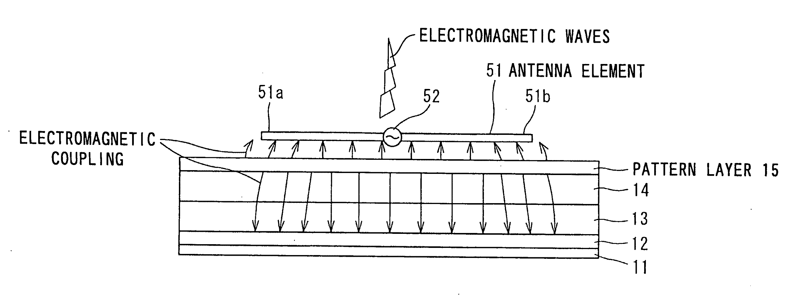
[0290]As the pattern layer 15 and the reflection area forming layer 12, aluminum-evaporated polyethylene terephthalate (polyethylene terephthalate: abbreviated to PET) having a thickness of 100 μm was used. The layer thickness of the aluminum layer in the pattern layer 15 and the reflection area forming layer 12 is 100 μm. The pattern layer 15 was produced by evaporating aluminum on PET to form an aluminum layer, and etching this aluminum layer to form a pattern shape shown in FIG. 19. The first storage layer 14 was produced using a method in which 100 parts by weight of SBS (styrene / butadiene / styrene copolymer) resin, 35 parts by weight of carbon black as a dielectric material, 205 parts by weight of ferrite as a magnetic material, and a dispersant (no magnetic member was used) were mixed, kneaded, and formed into a sheet having a thickness of 1 mm by extrusion molding. The second storage layer 13 was produced as a sheet having a thickness of 1.75 mm in which red phosphorus and mag...

example 2

[0292]As the pattern layer 15 and the reflection area forming layer 12, aluminum-evaporated polyethylene terephthalate (PET) having a thickness of 100 μm was used. The layer thickness of the aluminum layer in the pattern layer 15 and the reflection area forming layer 12 is 0.05 μm. The pattern layer 15 was produced by evaporating aluminum on PET to form an aluminum layer, and etching this aluminum layer to form a pattern shape shown in FIG. 28. The first storage layer 14 was produced using a method in which 100 parts by weight of PVC (KANEKA CORPORATION, KS1700) resin, 80 parts by weight of DOP [dioctyl phthalate (phthalic acid di-2-ethylhexyl) 1,2-benzenedicarboxylic acid bis(2-ethylhexyl)ester], 43 parts by weight of graphite as a dielectric material, 125 parts by weight of ferrite as a magnetic material, and calcium carbonate were mixed, kneaded, and formed into a sheet having a thickness of 0.3 mm by extrusion molding. The second storage layer 13 was produced as a sheet having a...

example 3

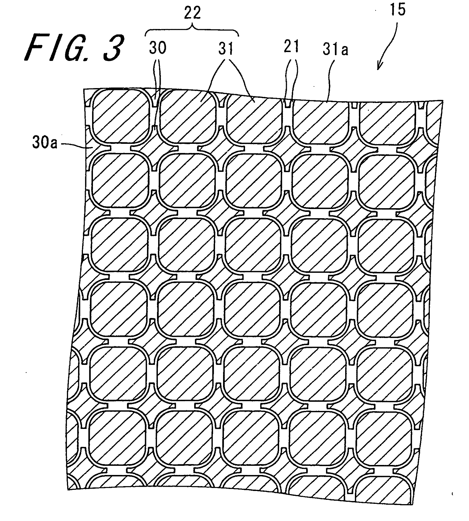
[0294]The pattern layer 15 was formed into a pattern shape shown in FIG. 22, and other procedures in the method were the same as those in Example 1.

[0295]Regarding the conductive pattern portions 22 of the pattern layer 15, b1x=b1y=21.0 mm, and d1x=d1y=1.5 mm. When the x direction of the conductive pattern portions 22 of the pattern layer 15 is set to the longer-side direction, and the y direction is set to the shorter-side direction, the rectangular pattern shapes 31a are arranged in the longer-side direction so that each of the centroids matches the center in shorter-side direction.


PUM


Abstract

In one embodiment of the present invention, a conductive pattern portion formed in a pattern layer functions as an antenna, and, when electromagnetic waves at a predetermined frequency arrive, resonance occurs, and an electromagnetic wave of a specific frequency is introduced into a sheet member. As to the sheet member having the pattern layer, even in a small and thin sheet member, the phase of reflected waves from the reflection area can be adjusted, and thus an area having high electric field intensity due to interference between reflected waves from the reflection area and arriving electromagnetic waves can be set in the vicinity of the antenna element. When the sheet member is disposed between an antenna element and a communication jamming member, an electromagnetic field is generated around the conductive pattern portion, and an electromagnetic energy is supplied from the conductive pattern portion to the antenna element, and therefore receiving power of the antenna element can be increased. Accordingly, wireless communication can be suitably performed.

Description

PRIORITY PARAGRAPH[0001]This application is the national phase under 35 U.S.C. §371 of PCT International Application No. PCT / JP2006 / 321087 which has an International filing date of Oct. 23, 2006, which designated the United States of America, and which claims priority on Japanese patent application number 2005-307325 filed Oct. 21, 2005, the entire contents of each of which are hereby incorporated herein by reference.TECHNICAL FIELD[0002]The present invention relates to a sheet member for improving communication, used for performing wireless communication using an antenna element in the vicinity of a communication jamming member, and an antenna device and an electronic information transmitting apparatus provided therewith.BACKGROUND ART[0003]FIG. 51 is a simplified cross-sectional view showing a tag 1 according to a conventional technique. FIG. 51 shows the case of wireless communication using an electromagnetic induction system typically used for a 13.56 MHz band. An RFID (radio fr...

Claims


Application Information

Patent Timeline
Patent Type & Authority Applications(United States)
IPC IPC(8): H01Q1/38
CPCH01Q1/526H01Q15/0026H01Q19/108H01Q17/00
Inventor OKAMURA, HARUHIDEYOSHIDA, TAKAHIKOMATSUSHITA, MASATOKIYOHARA, YOSHIHARUSATO, SHINICHIYOSHIHARA, RYOTAMORITA, KAZUHISAKOGURE, HIROAKI
Owner NITTA CORP
Why Eureka
Try Eureka