Display device

a display device and display technology, applied in the field of display devices, can solve the problems of difficult stabilization of differential current i, difficulty in accurately corresponding to ambient light intensity, etc., and achieve the effect of accurately detecting ambient light intensity and reducing the error of ambient light detection

Inactive Publication Date: 2010-03-11
SHARP KK
View PDF28 Cites 7 Cited by
  • Summary
  • Abstract
  • Description
  • Claims
  • Application Information

AI Technical Summary

Benefits of technology

[0058]According to this invention, (i) the first regions where the respective first photoelectric conversion devices are provided and (ii) the second regions where the respective second photoelectric conversion devices are provided are separately provided so as to be alternated in the surface of the display panel. Therefore, an average of the characteristics of all of the respective first regions is obtained as representative characteristics of the first photoelectric conversion devices; an average of the characteristics of all of the respective second regions is obtained as representative characteristics of the second photoelectric conversion devices. Therefore, (i) the representative characteristics of the first photoelectric conversion devices and (ii) the representative characteristics of the second photoelectric conversion devices can be almost equalized. This applies even in a case where there is a great variation in the characteristics of the photoelectric conversion devi...

Problems solved by technology

However, in a case where the differential current ΔI is obtained at certain bias points of curved lines adjacent to each other, as the curved lines c1 and c2 in FIG. 9, the differential current ΔI is difficult to accurately correspond to the intensity of the ambient light AL because an output current indicated by the curved line c1, which...

Method used


Image

  • Display device
  • Display device
  • Display device

Examples


Embodiment Construction

[0135]One embodiment of the present invention is described below with reference to FIG. 1 through FIG. 7, and FIG. 22.

[0136]FIG. 3 shows a liquid crystal display device 1 according to the present embodiment.

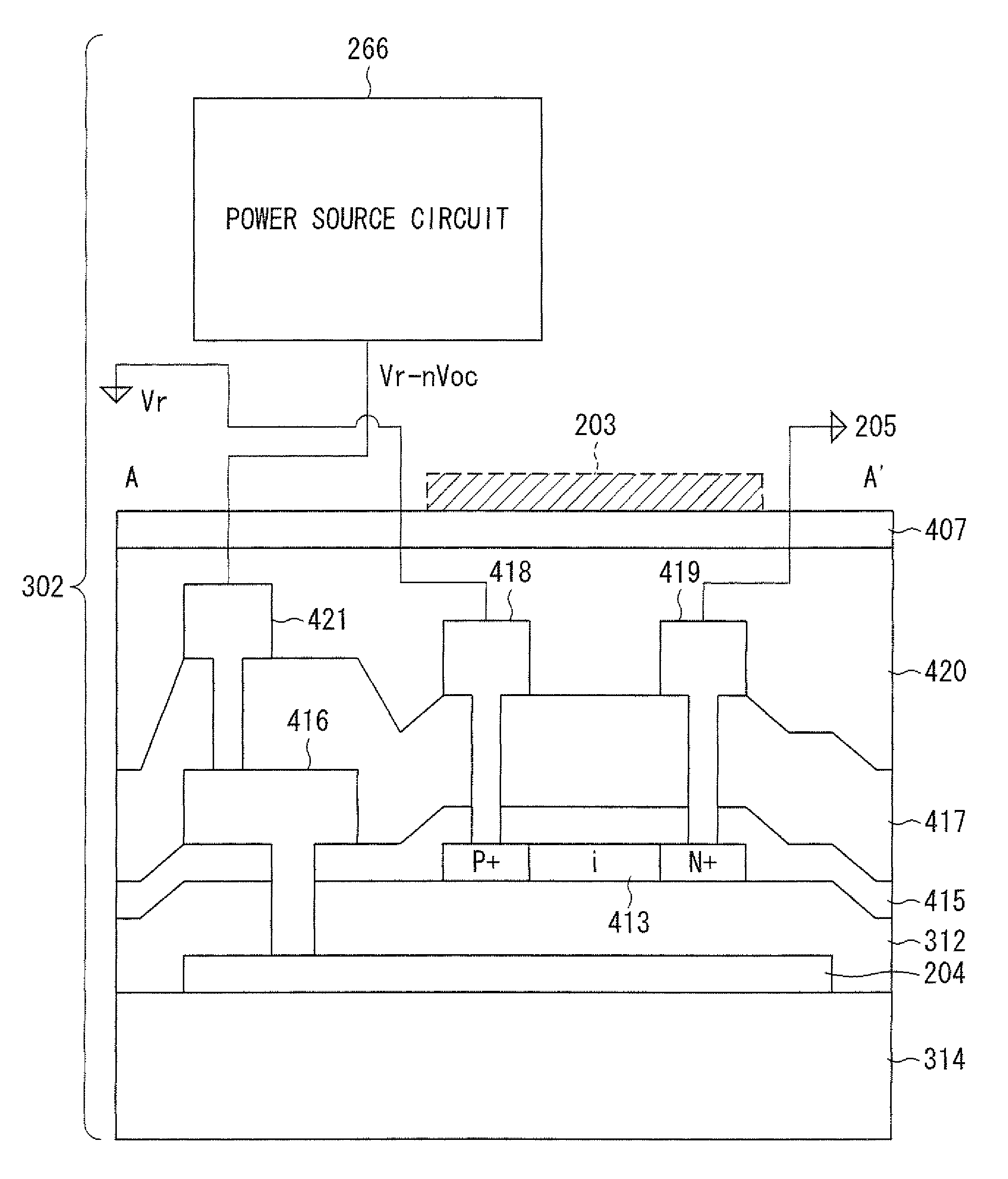
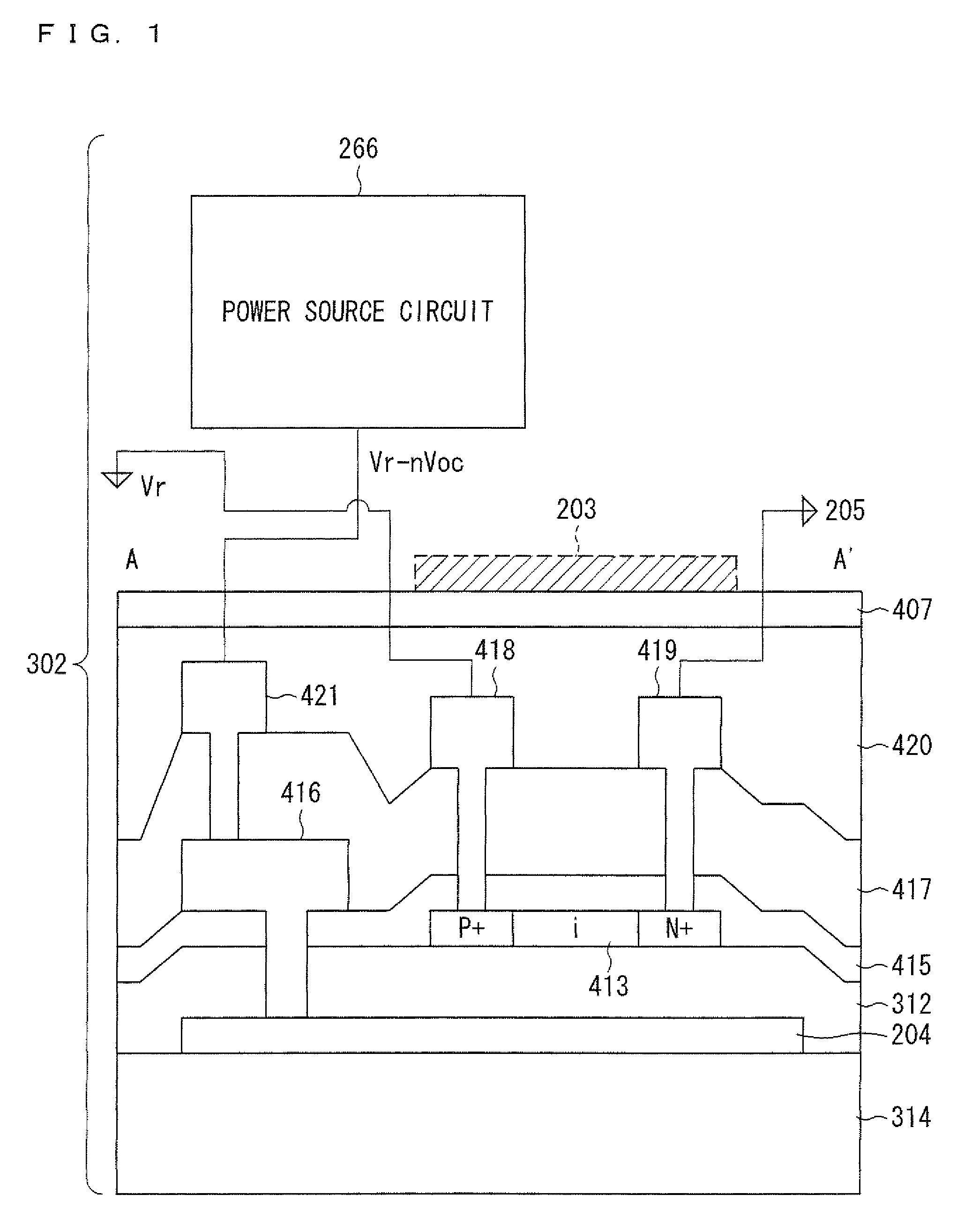
[0137]The liquid crystal display device 1 is realized by modifying the liquid crystal display device 250 illustrated in FIG. 14 in such a manner that (i) the layout and the respective configurations of the detecting device (first photoelectric conversion device) 201 and the reference device (second photoelectric conversion device) 202 of the ambient light sensor are changed, (ii) the configuration of the wiring 265 including the wiring connected with the detecting device 201 and the wiring connected with the reference device 202 is changed, and (iii) a power source circuit 266 is additionally provided. A pixel configuration of a matrix display section 261 is the same as that illustrated in FIG. 15.

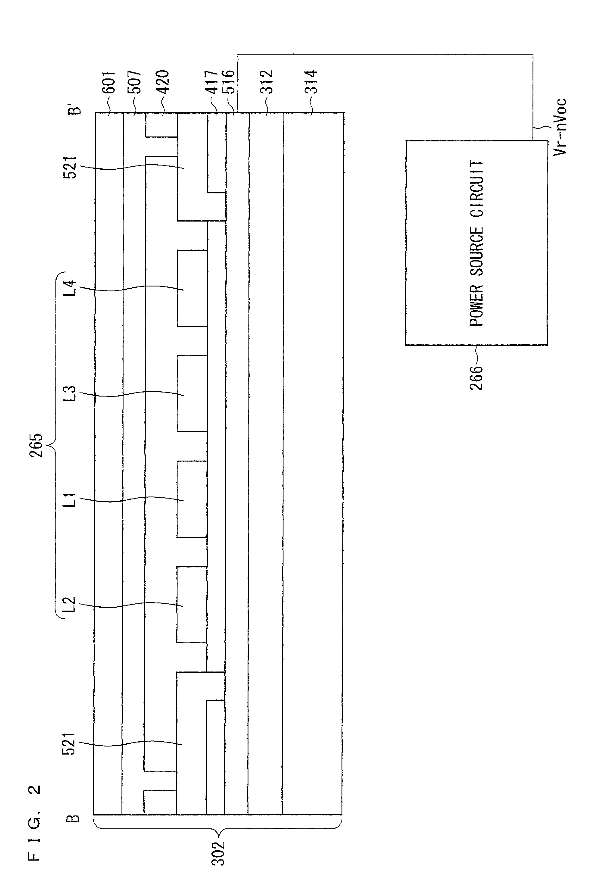
[0138]FIG. 4 shows a configuration of an ambient light sensor of a liquid crystal d...


PUM


Abstract

In a liquid crystal display device (1), (i) regions where respective detecting devices (201) are provided and (ii) regions where respective reference devices (202) are provided are separately arranged so as to be alternated along a frame. In each region, a predetermined number of PIN photodiodes (413) are connected in series and in parallel. In the whole of the first regions, (i) a series connection of n PIN photodiode(s) and (ii) a predetermined number of parallel connections are provided; in the whole of the second regions, (i) a series connection of n PIN photodiode(s) and (ii) a predetermined number of parallel connections are provided. Thus, even in a case where there is a great variation in the characteristics of photoelectric conversion device elements in a display panel which photoelectric conversion device elements configure a photoelectric conversion device, an intensity of ambient light can be detected accurately in the display device.

Description

TECHNICAL FIELD[0001]The present invention relates to a display device including an ambient light sensor.BACKGROUND ART[0002]As portable terminals (e.g., a mobile phone and a PDA) provided with a liquid crystal display, the ones including an ambient light sensor system are widely used, the ambient light sensor system adjusting a luminance of a backlight of the liquid crystal display in accordance with a brightness of its surroundings. In a display capable of transmissive liquid crystal mode operation, the ambient light sensor system detects an intensity of ambient light by means of an ambient light sensor provided in the peripheral of a panel. If the intensity of the ambient light is weak, the ambient light sensor system reduces the luminance of the backlight; if the intensity of the ambient light is strong, the ambient light sensor system increases the luminance of the backlight. By carrying out this control, the ambient light sensor system provides a user with a comfortable view. ...

Claims


Application Information

Patent Timeline
IPC IPC(8): G01J1/32
CPCG01J1/1626G01J1/4204G01J1/4228G01J1/44G09G2360/144G02F1/133604G02F2201/58G09G3/3406G02F1/133603
Inventor SATOH, MASAKAZUKATOH, HIROMIHADWEN, BENJAMIN JAMES
Owner SHARP KK
Why Eureka
Try Eureka