
Semiconductor light-emitting apparatus

a technology of light-emitting apparatus and semiconductor, which is applied in the direction of electrical apparatus, semiconductor/solid-state device manufacturing, and semiconductor devices. it can solve the problems of not being able to enhance light-emitting efficiency by adjusting the geometric dimension, and the optical self-absorption of the light-emitting device can be reduced, and the light-emitting apparatus can be enhanced. the effect of light-emitting apparatus light-emitting efficiency and enhanced light-emi

Inactive Publication Date: 2010-03-11
SHOWA DENKO KK
View PDF1 Cites 18 Cited by
  • Summary
  • Abstract
  • Description
  • Claims
  • Application Information

AI Technical Summary

Benefits of technology

The present invention provides a light-emitting apparatus that reduces optical self-absorption and enhances light extraction efficiency. This is achieved by tilting the side surface of the encapsulating structure with respect to the bottom of the semiconductor light-emitting device. The light-emitting apparatus also has the ability to disperse light or concentrate it on the front, which can be achieved by designed a specific distance between the light-emitting device and the top and bottom of the encapsulating structure. The light-emitting apparatus is easy to produce and has improved performance.

Problems solved by technology

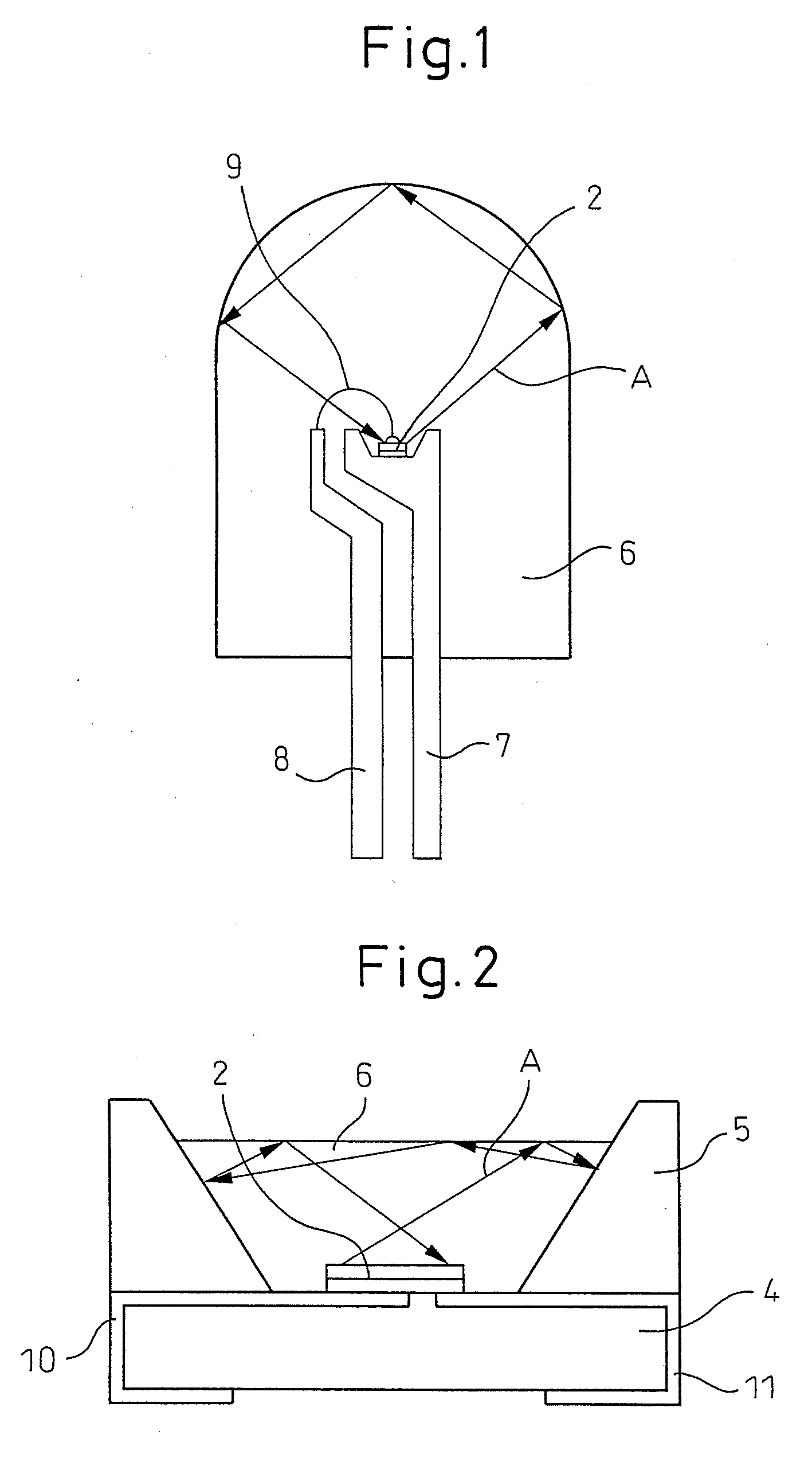
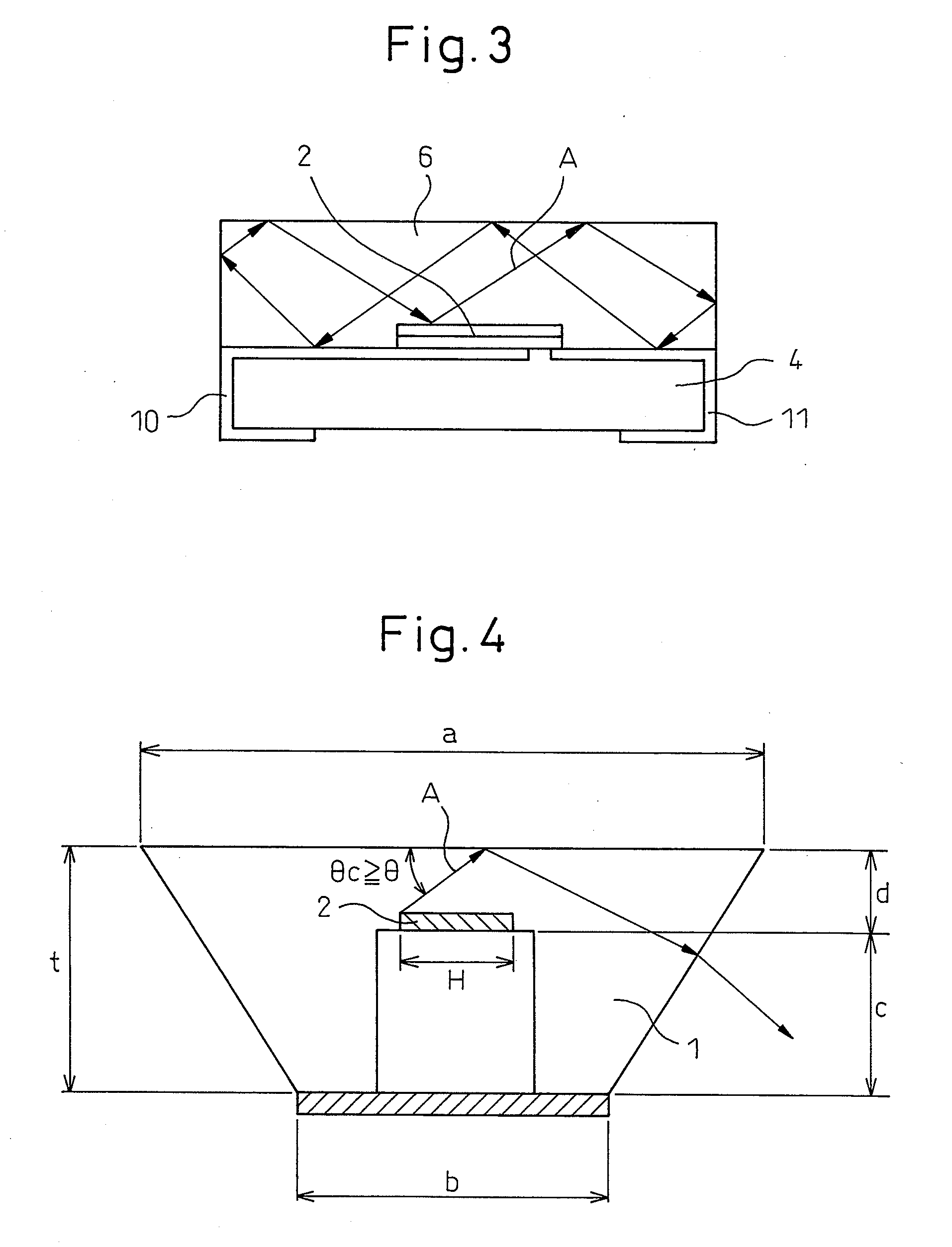
In addition, in the configuration of FIG. 3, the main purpose is so that energization of a device can be confirmed by lighting of the light-emitting device, and productivity of the light-emitting apparatus is important, but the light extraction is not improved.
However, in the light-emitting apparatus loaded with a light-emitting device, it is not known to enhance light extraction efficiency by adjusting the geometric dimension.

Method used


Image

  • Semiconductor light-emitting apparatus
  • Semiconductor light-emitting apparatus
  • Semiconductor light-emitting apparatus

Examples


example 1

[0102]First Example of the light-emitting apparatus related to the present invention is described in detail below by referring to the drawings. FIG. 14 is a cross-sectional view of the light-emitting apparatus produced in this Example, and FIG. 15 is a plan view of the light-emitting apparatus. The light-emitting apparatus 111 is composed of a heat-radiating substrate 104, a submount 103, a semiconductor light-emitting device 102 and an encapsulating structure 101. Also, 120 is an electrode for external power supply connection, and 121 is a worked part for heat sink attachment.

[0103]The semiconductor light-emitting device 102 used is the following flip-chip type GaN-based compound semiconductor blue light-emitting device having a square shape with a side length of 0.35 mm×0.35 mm and having a thickness of about 90 μm. This light-emitting device is a light-emitting device obtained by sequentially stacking a 8 μm-thick underlying layer composed of undoped GaN, a 2 μm-thick Ge-doped n-...

example 2

[0115]In this Example, a light-emitting apparatus was produced in the same manner as in Example 1 except that the outer diameter of the top of the ring-like tapered tube was 0.8 mm. Accordingly, the ratio of the outer diameter between the top and the bottom of the encapsulating structure of this Example was (0.8 / 1.6=0.5), and the area ratio therebetween was ((0.8)2 / (1.6)2=0.25). FIG. 16 is a cross-sectional view of the light-emitting apparatus produced in this Example, and FIG. 17 is a plan view thereof.

[0116]The thus-obtained light-emitting apparatus was subjected to an energization test. The voltage was 3.2 V at an input current of 20 mA. The output of the light-emitting apparatus was 17.91 mW and the ratio of the output to the input energy was 27.98%. Also, the front light intensity at this time was 0.004 [W / sr]. Furthermore, the light extraction quantity of the light-emitting apparatus of this Example was 1.64 times the light extraction quantity of the light-emitting device in a...

example 3

[0119]In this Example, a light-emitting apparatus was produced in the same manner as in Example 1, except that the outer diameter of the top of the ring-like tapered tube was 2.4 mm. Accordingly, the ratio of the outer diameter between the top and the bottom of the encapsulating structure of this Example was (2.4 / 1.6=1.5), and the area ratio therebetween was ((2.4)2 / (1.6)2=2.25).

[0120]The thus-obtained light-emitting apparatus was subjected to an energization test. The voltage was 3.2 V at an input current of 20 mA. The output of the light-emitting apparatus was 18.14 mW and the ratio of the output to the input energy was 28.34%. Also, the front light intensity at this time was 0.0019 [W / sr]. Furthermore, the light extraction quantity of the light-emitting apparatus of this Example was 1.65 times the light extraction quantity of the light-emitting device in a bare chip state.


PUM


Abstract

An object of the present invention is to provide a light-emitting apparatus reduced in the optical self-absorption of the light-emitting device and assured of excellent light extraction efficiency. The inventive light-emitting apparatus comprises a substrate, a semiconductor light-emitting device provided on the substrate with or without intervention of a submount, and an encapsulating structure for encapsulating the semiconductor light-emitting device, wherein the encapsulating structure has a bottom parallel to the bottom of the semiconductor light-emitting device and the side surface of the encapsulating structure is tilted with respect to the bottom.

Description

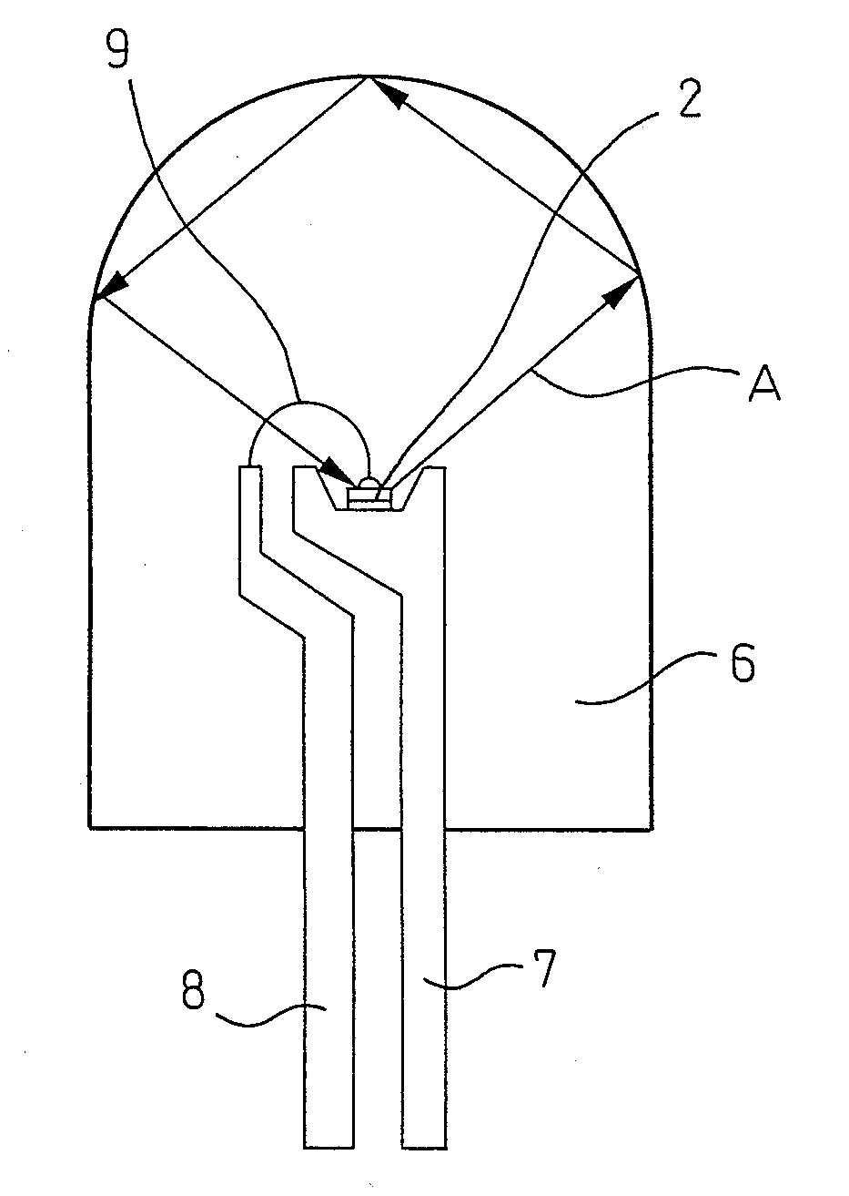
TECHNICAL FIELD[0001]The present invention relates to a semiconductor light-emitting apparatus. More specifically, the present invention relates to a semiconductor light-emitting apparatus assured of excellent light extraction efficiency and enabled to control the radiation dispersibility of light, in which, in order to reduce optical self-absorption of the semiconductor light-emitting device, the side surface of an encapsulating structure is tilted with respect to the bottom and a specific distance is arranged between a semiconductor light-emitting device and the top and bottom of the encapsulating structure.BACKGROUND ART[0002]As for the light-emitting apparatus using a semiconductor light-emitting device, there have been conventionally known, for example, a light-emitting apparatus where as shown in FIG. 1, a light-emitting device is mounted on a lead frame and the entirety is resin-encapsulated in a cannonball shape, and a light-emitting apparatus where as shown in FIG. 2, a ref...

Claims


Application Information

Patent Timeline
Patent Type & Authority Applications(United States)
IPC IPC(8): H01L33/00H01L21/56H01L33/48H01L33/54
CPCH01L33/486H01L33/54H01L2224/32257H01L2224/48091H01L2224/48247H01L2224/73265H01L2924/01322H01L2924/00014H01L2924/00
Inventor HOSHINA, TAKAHARU
Owner SHOWA DENKO KK
Learn More