Trench gate type transistor and method of manufacturing the same

Active Publication Date: 2010-03-11
SEMICON COMPONENTS IND LLC
View PDF8 Cites 17 Cited by
  • Summary
  • Abstract
  • Description
  • Claims
  • Application Information

AI Technical Summary

Benefits of technology

[0014]The trench gate type transistor and the method of manufacturing the same of the invention reduce the

Problems solved by technology

Furthermore, since the trench is round from the bottom surface to the sidewall, the semiconductor layer near the trenc

Method used


Image

  • Trench gate type transistor and method of manufacturing the same
  • Trench gate type transistor and method of manufacturing the same
  • Trench gate type transistor and method of manufacturing the same

Examples


first embodiment

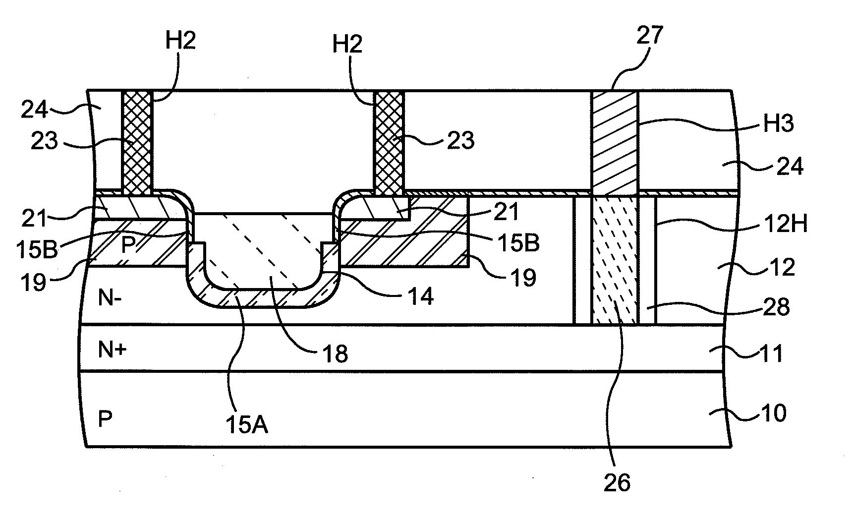
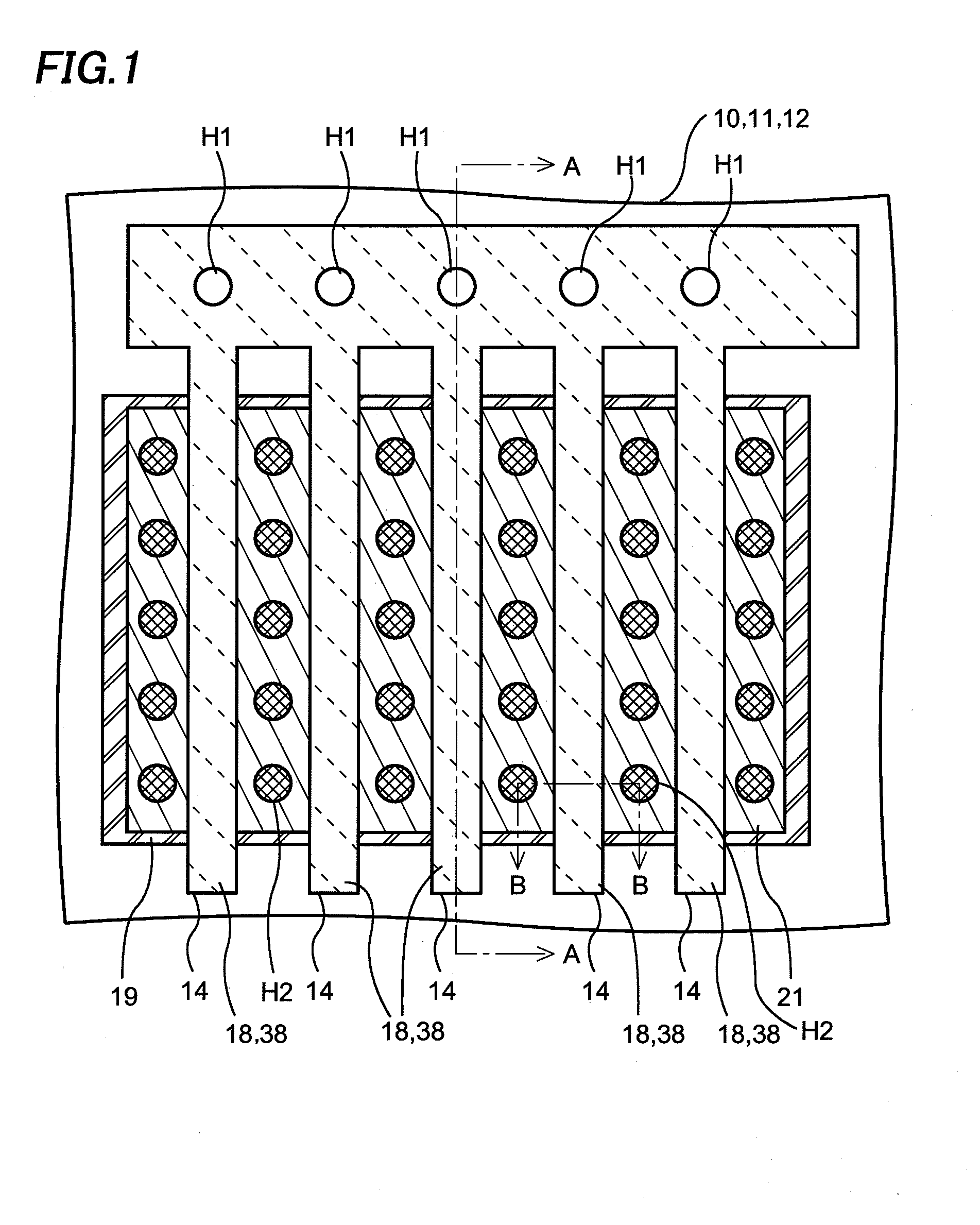
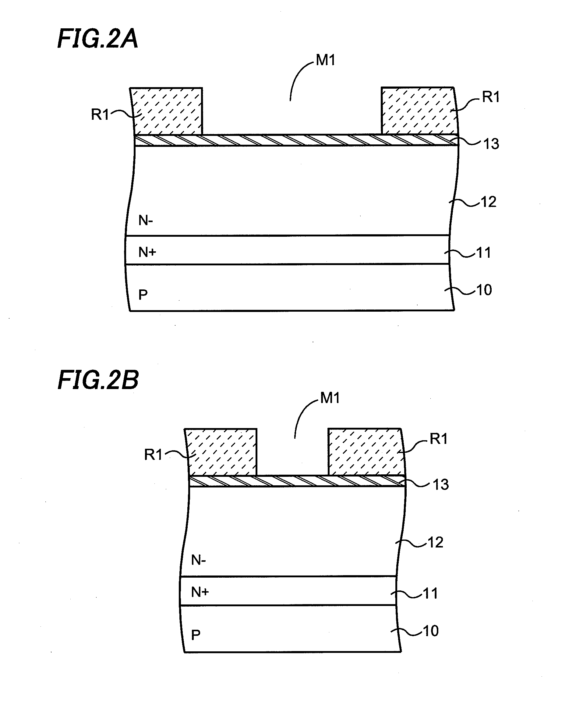
[0019]A first embodiment of the invention will be described referring to figures. FIG. 1 is a plan view for explaining a trench gate type transistor and a method of manufacturing the same of the embodiment of the invention. FIGS. 2(A) to 14(A) are cross-sectional views of FIG. 1 along line A-A, and FIGS. 2(B) to 14(B) are cross-sectional views of FIG. 1 along line B-B. In the following description, the trench gate type transistor is referred to as a transistor simply. The conductive type of this transistor is not limited, but the following description is given for a case of an N channel type transistor.

[0020]First, the schematic plan structure of the transistor of the embodiment will be described referring to FIG. 1. Here, only main elements will be described. In this transistor, an N+ type semiconductor layer 11 and an N− type semiconductor layer 12 are formed on a P type semiconductor substrate 10, and a plurality of trenches 14 each having short sides and long sides is formed in ...

second embodiment

[0043]A second embodiment of the invention will be described referring to figures. The schematic plan structure of this transistor is the same as that of FIG. 1.

[0044]Hereafter, a trench gate type transistor and a method of manufacturing the same of the embodiment will be described referring to figures. FIGS. 17(A) to 26(A) are cross-sectional views of FIG. 1 along line A-A, and FIGS. 17(B) to 26(B) are cross-sectional views of FIG. 1 along line B-B. In FIGS. 17 to 26, the same numerals are given to the same elements as those of FIGS. 2 to 14.

[0045]First, in the similar manner to the processes shown in FIGS. 2 to 5 in the first embodiment, an N+ type semiconductor layer 11 and an N− type semiconductor layer 12 are formed on a semiconductor substrate 10, and trenches 14 are formed in the N− type semiconductor layer 12. A silicon oxide film 35A which corresponds to the silicon oxide film 15A, and a photoresist reinforcement film 36 which corresponds to the photoresist reinforcement fi...


PUM


Abstract

The invention provides a trench gate type transistor in which the gate capacitance is reduced, the crystal defect is prevented and the gate breakdown voltage is enhanced. Trenches are formed in an N− type semiconductor layer. A uniformly thick silicon oxide film is formed on the bottom of each of the trenches and near the bottom, being round at corner portions. A silicon oxide film is formed on the upper portion of the sidewall of each of the trenches, which is thinner than the silicon oxide film and round at corner portions. Gate electrodes are formed from inside the trenches onto the outside thereof. The thick silicon oxide film reduces the gate capacitance, and the thin silicon oxide film on the upper portion provides good transistor characteristics. Furthermore, with the round corner portions, the crystal defect does not easily occur, and the gate electric field is dispersed to enhance the gate breakdown voltage.

Description

REFERENCE TO RELATED APPLICATIONS[0001]This application is a national stage application under 35 USC 371 of International Application No. PCT / JP2008 / 068116, filed Sep. 26, 2008, which claims priority from Japanese Patent Application No. 2007-255091, filed Sep. 28, 2007, the contents of which are incorporated herein by reference.BACKGROUND OF THE INVENTION[0002]1. Field of the Invention[0003]The invention relates to a trench gate type transistor and a method of manufacturing the same.[0004]2. Description of the Related Art[0005]A DMOS transistor is a double-diffused MOS field effect transistor and used as a power semiconductor device for a power supply circuit, a driver circuit or the like. A trench gate type transistor is known as a type of DMOS transistor.[0006]This trench gate type transistor is configured by forming a gate insulation film 115 in a trench 114 formed in a semiconductor layer 112 and forming a gate electrode 116 covering the gate insulation film 115 in the trench 11...

Claims


Application Information

Patent Timeline
IPC IPC(8): H01L29/78H01L21/336
CPCH01L29/4238H01L29/66734H01L29/7809H01L29/7813H01L29/42368H01L29/0696H01L29/41741H01L29/41766H01L29/4236H01L29/0653
Inventor SHIMADA, SATORUYAMAOKA, YOSHIKAZUFUJITA, KAZUNORITABE, TOMONORI
Owner SEMICON COMPONENTS IND LLC
Why Eureka
Try Eureka