Stamper for minute structure transfer and a method for manufacturing the same

a technology of minute structure and stamper, which is applied in the direction of photomechanical equipment, applications, instruments, etc., can solve the problems of reducing internal stress and not being able to curve the nickel stamper at more than, and achieve excellent durability

Inactive Publication Date: 2010-03-11
HITACHI CABLE
View PDF11 Cites 34 Cited by
  • Summary
  • Abstract
  • Description
  • Claims
  • Application Information

AI Technical Summary

Benefits of technology

[0014]Thus, the present invention can provide a stamper for minute structure transfer and a method for manufacturing the same as being excellent in durability.

Problems solved by technology

As the thermal contraction sheet includes the resin, it is not able to curve the Nickel stamper at more than or equal to glass transition temperature.
As the Nickel stamper is curved only by an internal stress of Nickel, after the thermal contraction sheet has been removed, it has a problem to reduce the internal stress and return to be flat in the Nickel stamper, when the Nickel stamper is repeated to heat up and refrigerate in the process of minute structure transfer.

Method used


Image

  • Stamper for minute structure transfer and a method for manufacturing the same
  • Stamper for minute structure transfer and a method for manufacturing the same
  • Stamper for minute structure transfer and a method for manufacturing the same

Examples


example 1

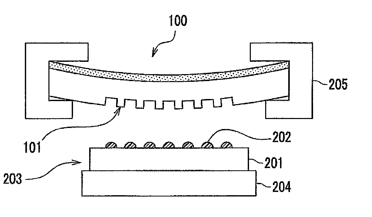
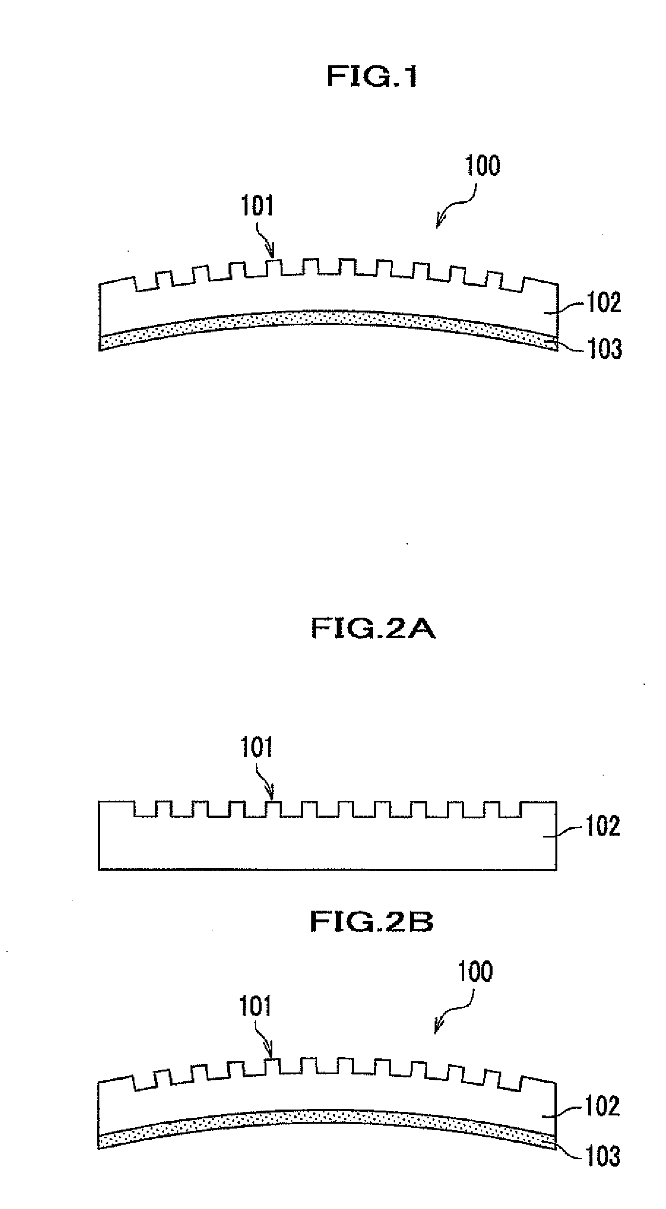
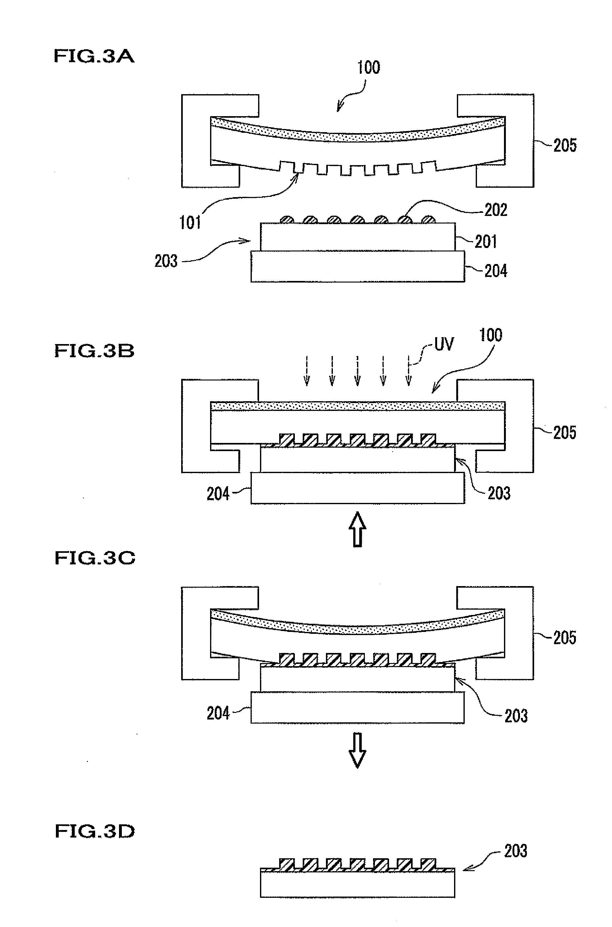
[0073]In this example, the stamper 100 has been manufactured by a method as shown in FIGS. 2A and 2B.

[0074]As the substrate 102, the substrate made of quartz having 100 mm in diameter, 0.5 mm in thickness, and 5.4×10⁻⁷° C.−1 in coefficient of linear expansion is used. At first, as shown in FIG. 2A, the minute pattern 101 is formed by the well-known photolithography technique on one side of the substrate 102 made of quartz. The minute pattern 101 is constituted to arrange a hole having 0.5 μm in diameter and 1 μm in depth with an interval between centers thereof being 1 μm. Next, as shown in FIG. 2B, the thin film 103, of which the principal component is SiO2, including GeO2 of 24 mol percentage, is manufactured by the well-known spattering technique in the side opposite to the side forming the minute pattern 101.

[0075]At this time, the substrate 102 is mounted inside the chamber of a film formation apparatus as not shown, the thin film 103 is constituted to control the time for film...

example 2

[0078]In this example, the stamper 100 has been manufactured by a method as shown in FIG. 4A to FIG. 4C.

[0079]A multi-component glass substrate including the flat fluoride having 100 mm in diameter, 0.5 mm in thickness, and 32×10−7° C.−1 in coefficient of linear expansion has been used.

[0080]As shown in FIG. 4A, the thin film 103 composing of SiO2 having 0.5 μm by the vacuum vapor technique is formed on both sides of the substrate 102 made of quartz. The thin films 103 existing on both sides are respectively formed at a temperature 250 degree C. to keep a flat property of the substrate 102.

[0081]Next, as shown in FIG. 4B, the minute pattern 101 is formed by the well-known photolithography on one side of the substrate 102 forming the thin film 103 existing on both sides.

[0082]This minute pattern 101 is constituted to arrange a hole having 0.5 μm in diameter and 1 μm in depth with an interval between centers being 1 μm.

[0083]Next, as shown in FIG. 4C, the thin film 103, as formed in t...

example 3

[0086]In this embodiment, the stamper 100 is manufactured by a method shown in FIG. 5A to FIG. 5D.

[0087]As the substrate 102, a substrate made of quartz having 100 mm in diameter, 0.5 mm in thickness, and 5.4×10⁻⁷° C.−1 in coefficient of liner expansion is used.

[0088]As shown in FIG. 5A, the thin film 103, of which the principal component is SiO2, including GeO2 of 24 mol percentages, with the thickness thereof being 0.1 μm, is formed by the spattering technique on both sides of the substrates 102. The thin films 103 existing on both sides are respectively formed at a temperature of 200 degrees C. to keep the flat property of the substrate 102.

[0089]Next, as shown in FIG. 5B, the minute pattern 502 (resist pattern) is transferred on one side of the thin film 103 by the well-known imprinting technique. The minute pattern 502 is concentrically arranged with a line having 50 nm in width and 50 nm in height (H1 as shown in FIG. 5B) and with a line of 50 nm being at a pitch of 100 nm bet...


PUM

PropertyMeasurementUnit
wavelengthaaaaaaaaaa
distanceaaaaaaaaaa

Abstract

The present invention can provide a stamper for minute structure transfer to be excellent in durability. The present invention is characterized by which a minute pattern as formed in one side of a substrate comes in contact with a material to be transferred and the minute pattern is transferred on a resin layer of a surface of the material to be transferred. At least one layer of a thin film is mounted on at least one side of both surfaces of the substrate, the substrate and the thin film are different in a coefficient of linear expansion each other, and the substrate is curved to swell up to be convex in the side of the minute pattern by an internal stress generated in the thin film.

Description

TECHNICAL FIELD [0001]The present invention relates to a stamper for minute structure transfer of a minute concave and convex configuration.BACKROUND ART [0002]Semiconductor integrated circuits have been made extremely smaller in recent years. To realize an extremely small manufacturing, for example, when a pattern formation of the semiconductor integrated circuit may be micro-fabricated by photolithography, a high degree of accuracy has been required. On the other hand, as a scale of the micro-fabrication has nearly reached a wavelength of an exposing source, the formation of a pattern with a high degree of accuracy has been approaching the limit. Then, to obtain an even higher accuracy, an electron beam writing apparatus, which is a kind of charged particle beam apparatus, has been used instead of a photolithography apparatus.[0003]However, in forming a pattern with the electron beam writing apparatus, it takes much time to expose or write a pattern with a collective exposing ligh...

Claims


Application Information

Patent Timeline
Patent Type & Authority Applications(United States)
IPC IPC(8): B29C59/02B44C3/02B44C1/22
CPCB29C33/38B29C35/0888B29C37/0053B29C2035/0827B82Y10/00B82Y40/00G03F7/0002
Inventor ANDO, TAKASHIKITANO, NOBUAKIMIYAUCHI, AKIHIROWASHIYA, RYUTAOHSONO, KAZUMASAHONGO, AKIHITOSHIOTA, TSUNEO
Owner HITACHI CABLE
Why Eureka
Try Eureka