Stage apparatus, exposure apparatus, and device fabricating method
a technology of exposure apparatus and device, which is applied in the direction of photomechanical treatment, printing, instruments, etc., can solve the problems of significant cost increase, and achieve the effect of minimizing any cost increase, and increasing cos
- Summary
- Abstract
- Description
- Claims
- Application Information
AI Technical Summary
Benefits of technology
Problems solved by technology
Method used
Image
Examples
Embodiment Construction
[0031]The following text explains embodiments of a stage apparatus, an exposure apparatus, and a device fabricating method according to the present invention, referencing FIG. 1 through FIG. 10.
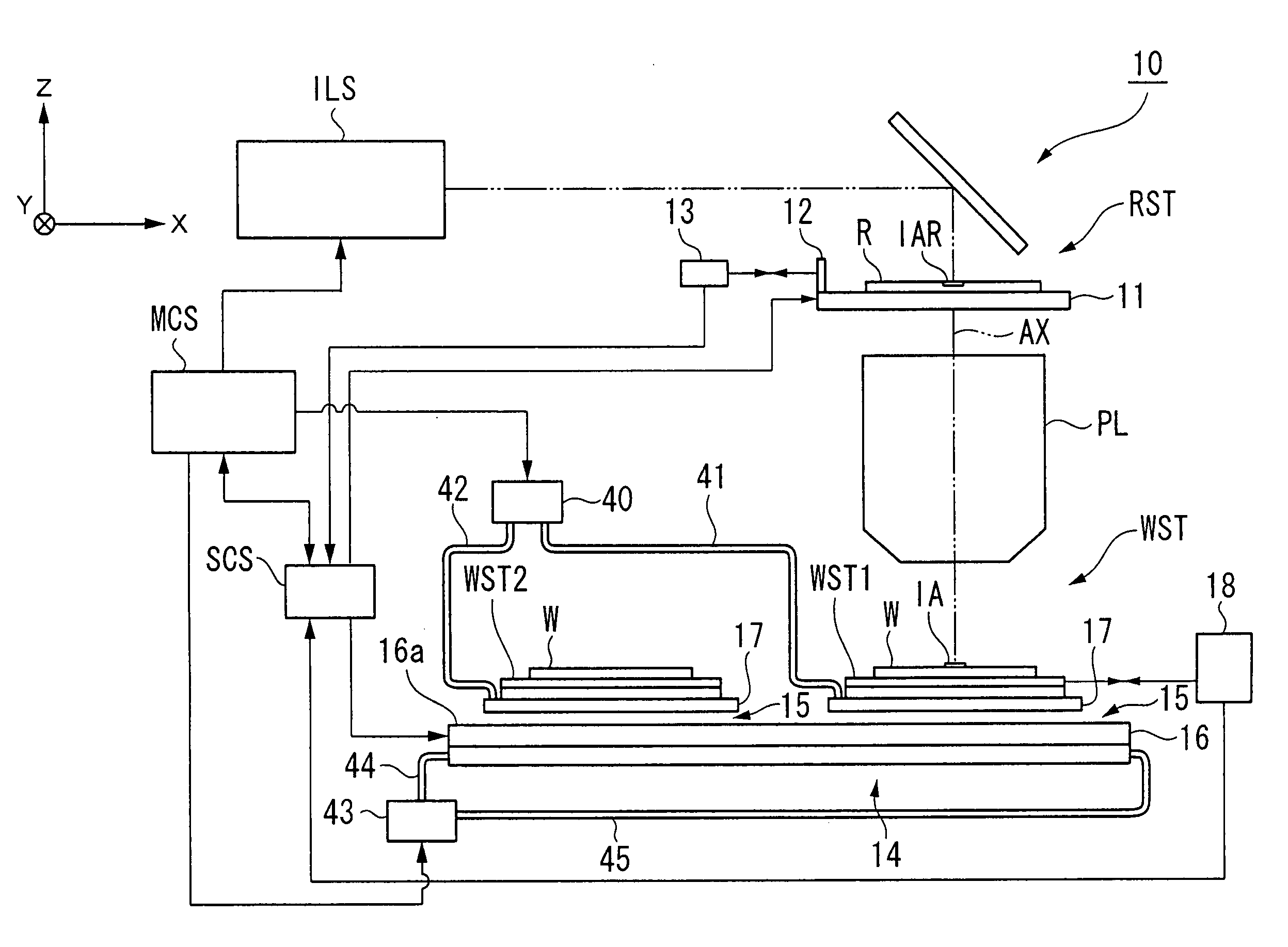
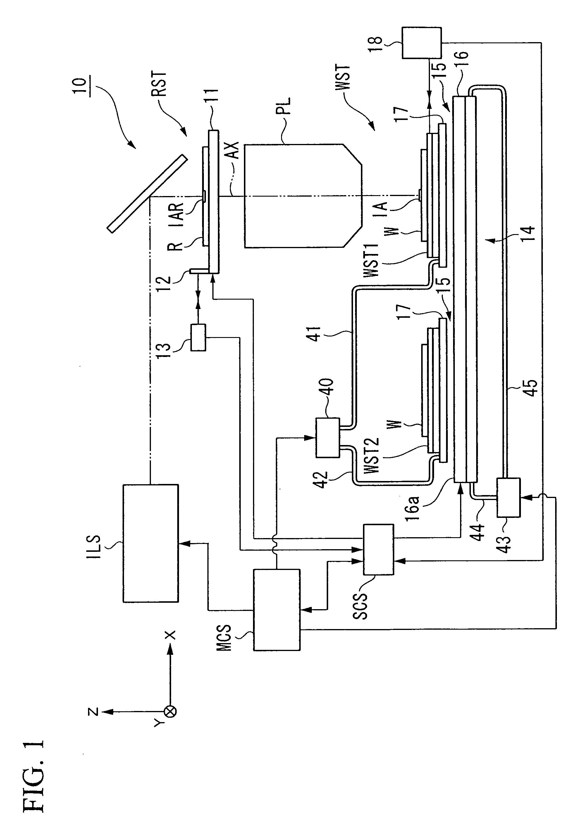
[0032]FIG. 1 is a schematic block diagram of the exposure apparatus according to one embodiment of the present invention. An exposure apparatus 10 shown in FIG. 1 is a step-and-scan type reduction projection type exposure apparatus for fabricating semiconductor devices that, while synchronously moving a reticle R (i.e., a mask) and a wafer W (i.e., a substrate), transfers a pattern, which is formed in the reticle R, successively onto the wafer W.
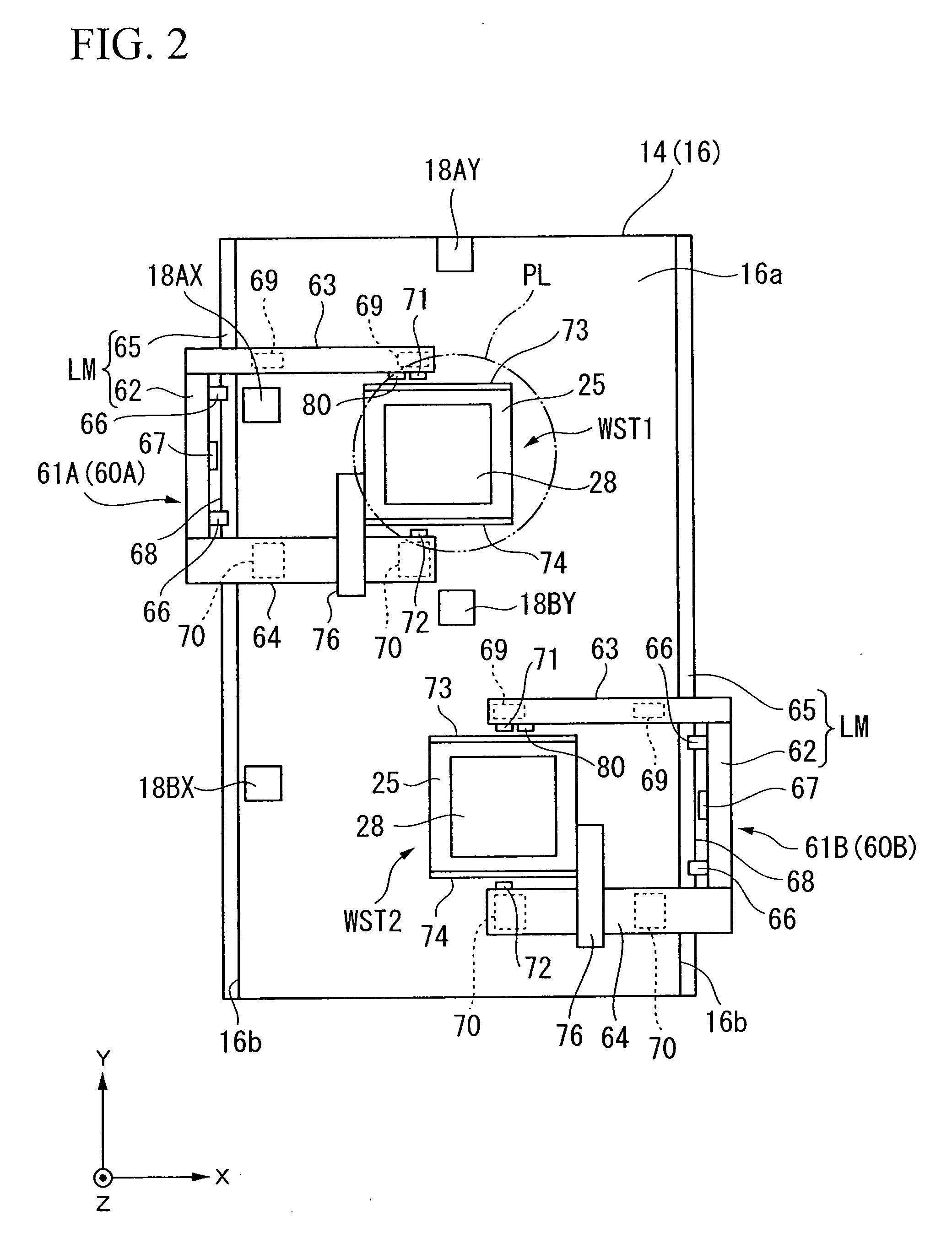
[0033]Furthermore, in the explanation below, an XYZ orthogonal coordinate system is defined in the figures where needed, and the positional relationships of members are described referencing this system. The XYZ orthogonal coordinate system is defined such that the X axis and the Z axis are parallel to the paper surface, and the Y axis is perpendicula...
PUM
 Abstract
Description
Claims
Application Information


