Defect detecting apparatus, defect detecting method, information processing apparatus, information processing method, and program therefor

a defect detection and defect technology, applied in the field of defect detection apparatus, information processing apparatus, information processing method, program therefor, can solve the problems of difficult maintenance or management of model image data, difficult preparation of absolutely normal products (models), and the likelihood of wrong detection of individual variations of defects, so as to achieve high accuracy and efficient detection of defects

Inactive Publication Date: 2010-03-18
TOKYO ELECTRON LTD
View PDF11 Cites 34 Cited by
  • Summary
  • Abstract
  • Description
  • Claims
  • Application Information

AI Technical Summary

Benefits of technology

[0045]In accordance with the present invention as described above, highly accurate and efficient detection of a defect of a MEMS device having a three-dimensional shape can be realized without having to use an absolute model image.

Problems solved by technology

Accordingly, prior to the creation of the model image data, a process for determining and selecting a normal product is required to be performed, and since this process needs to be performed manually, it takes much time and effort.
Further, in the inspection of the microstructures such as the MEMS devices in which a very minute flaw or foreign substance is regarded as a defect, preparing an absolutely normal product (model) is difficult in the aspect of maintenance or management of model image data.
Thus, in case that there are individual variations, resulted from a manufacturing process, in the respective inspection target objects, there is a likelihood that such individual variations would be wrongly detected as defects, though they are not actual defects but individual variations resulted from a manufacturing process.
As a result, inspection accuracy would be deteriorated.
Further, if the inspection target object has a height (thickness) in the direction of an optical axis of the image pickup camera, that is, if it has a three-dimensional shape, accurate recognition of a defect may not be possible even if the defect is present on the inspection target object because a captured image may become vague depending on an imaging focus, resulting in a failure to detect the defect.
Therefore, the technology of Patent Documents 3 can not be applied to an inspection of a device such as MEMS device for which obtaining a normal product image is difficult.

Method used


Image

  • Defect detecting apparatus, defect detecting method, information processing apparatus, information processing method, and program therefor
  • Defect detecting apparatus, defect detecting method, information processing apparatus, information processing method, and program therefor
  • Defect detecting apparatus, defect detecting method, information processing apparatus, information processing method, and program therefor

Examples


Embodiment Construction

[0046]Hereinafter, embodiments of the present invention will be described in detail with reference to the accompanying drawings.

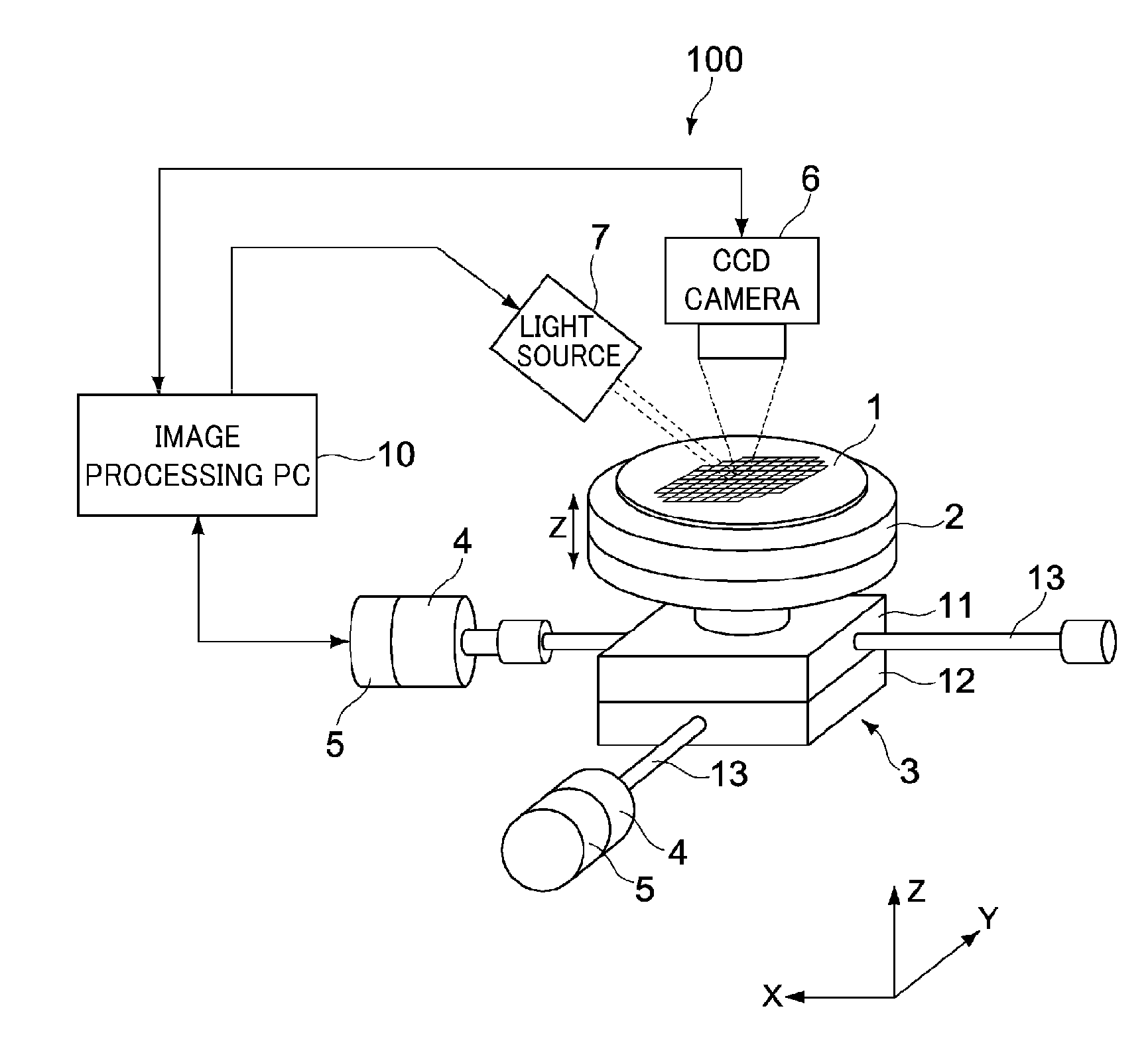
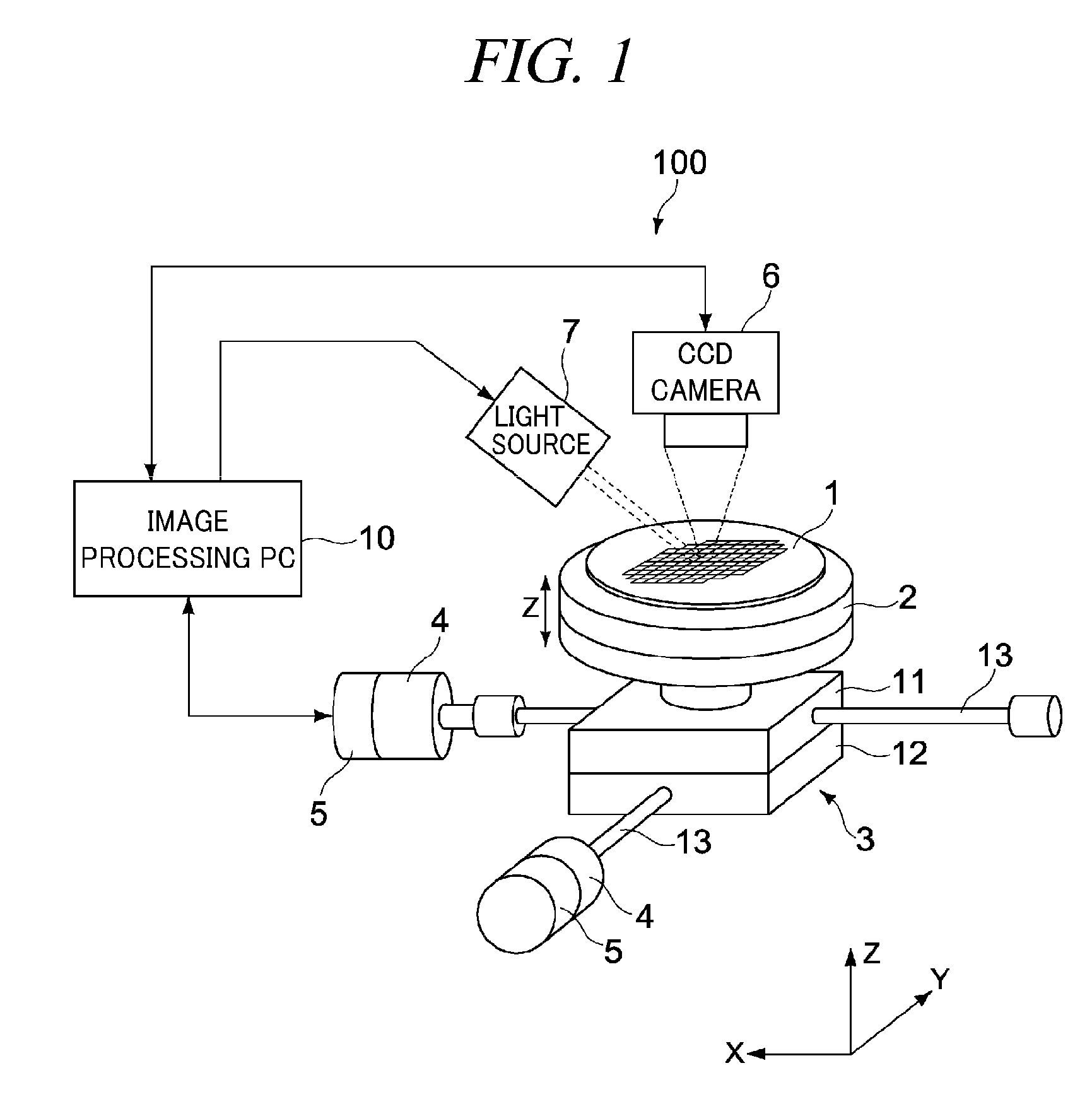
[0047]FIG. 1 is a configuration view of a defect detecting apparatus in accordance with an embodiment of the present invention. As illustrated in FIG. 1, the defect detecting apparatus 100 includes a wafer table 2 for holding thereon, e.g., a silicon semiconductor wafer 1 (hereinafter, simply referred to as a wafer 1); an XYZ stage 3 for moving the wafer table 2 along X, Y and Z directions of the figure; a CCD camera 6 for capturing an image of the wafer 1 from above; a light source 7 for illuminating the wafer 1 while the CCD camera 6 captures the image; an image processing PC (Personal Computer) 10 for controlling the operation of each component and performing image processing to be described later.

[0048]The wafer 1 is transferred onto the wafer table 2 by a non-illustrated transfer arm or the like and is attracted to and fixed on the wafer table 2 by, fo...


PUM


Abstract

A defect detecting apparatus captures images of a protein chip formed on each die of a wafer at a plurality of different focal positions, with respect to every division region obtained by dividing each die in plurality; stores inspection target images for every division region at every focal position together with an ID for identifying each division region; creates a model image for every division region at every focal position by calculating an average luminance value of pixels of each inspection target image having the corresponding ID; extracts a difference between the model image and each inspection target image as a difference image; extracts a Blob having an area larger than a preset value from each difference image as a defect; and classifies the kind of the defect based on a feature point of the extracted Blob.

Description

TECHNICAL FIELD [0001]The present invention relates to a defect detecting apparatus capable of detecting a defect such as a foreign substance, a flaw, and the like by performing a visual inspection of a microstructure such as MEMS (Micro Electro Mechanical Systems) formed on a semiconductor wafer, and also relates to a defect detecting method, an information processing apparatus, an information processing method, and a program to be used therefor.BACKGROUND ART [0002]Recently, MEMS devices, which integrate various functions in mechanical, electronic, optical and chemical field by using a micro-fabrication technology or the like, are attracting attention. As examples of MEMS device that have been in practical use so far, there are various sensors such as an acceleration sensor, a pressure sensor, an air flow sensor, and the like, which are used in an automobile or a medical field. In particular, MEMS devices are applied to a print head used in an inkjet printer, a micro mirror array ...

Claims


Application Information

Patent Timeline
Patent Type & Authority Applications(United States)
IPC IPC(8): G06K9/00
CPCB81C99/005G06T2207/30148G06T7/001G01N21/95607G01B11/30G01N21/956G06T1/00
Inventor KAWARAGI, HIROSHI
Owner TOKYO ELECTRON LTD
Why Eureka
Try Eureka