
Substrate structures applied in flexible electrical devices and fabrication method thereof

Active Publication Date: 2010-03-18
IND TECH RES INST
View PDF5 Cites 44 Cited by
  • Summary
  • Abstract
  • Description
  • Claims
  • Application Information

AI Technical Summary

Benefits of technology

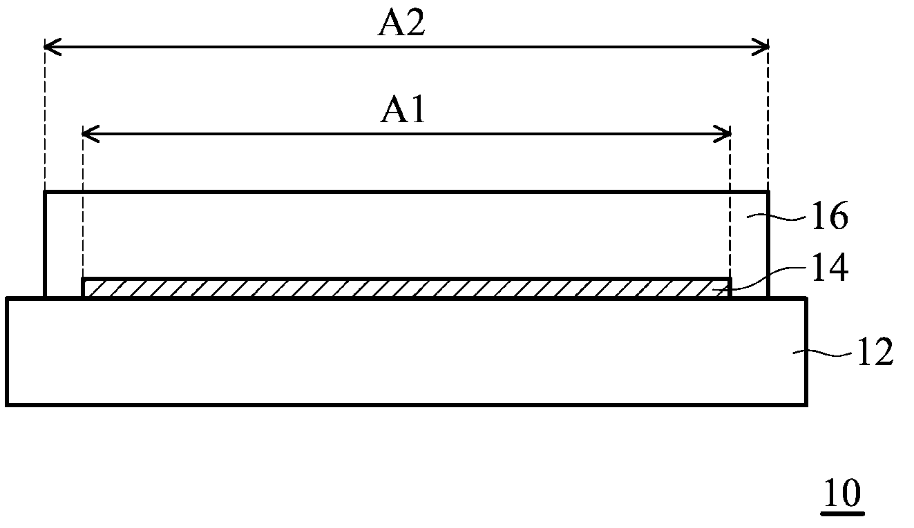
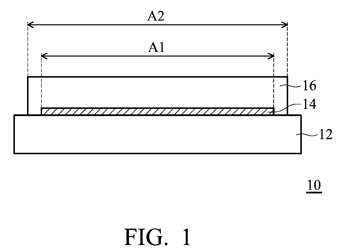
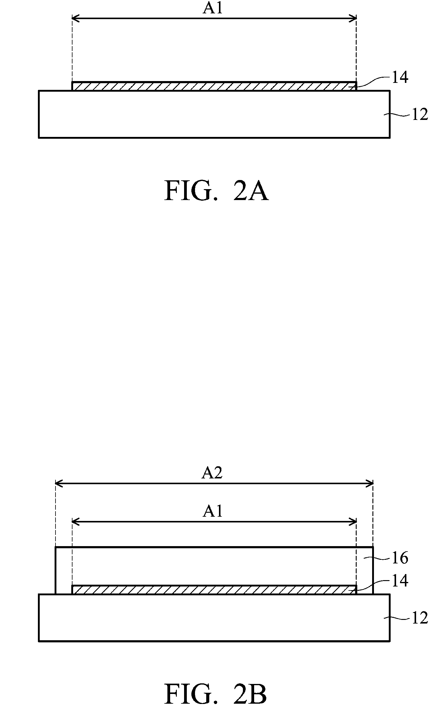
[0010]The substrate structure applied in flexible electrical devices provided by the invention is simply fabricated using present semiconductor apparatuses, characterized by various adhesion forces of the two release layers to the carrier. A release layer with lower adhesion force is first formed on the carrier with a smaller area. Another release layer with greater adhesion force (such as flexible

Problems solved by technology

However, development of substrate transfer and film separation techniques is required.

Method used


Image

  • Substrate structures applied in flexible electrical devices and fabrication method thereof
  • Substrate structures applied in flexible electrical devices and fabrication method thereof
  • Substrate structures applied in flexible electrical devices and fabrication method thereof

Examples


example 1

Preparation of parylene Release Layer

[0028]A parylene precursor (parylene dimer) was put into a thermal evaporation apparatus. A clean glass (15 cm×15 cm) covered with a hollow pad (8 cm×8 cm) was placed in a sample room. The parylene precursor was vaporized at 150° C. and decomposed at 650° C. in a vacuum and then conducted into the sample room. Parylene was deposited on the area uncovered by the pad at room temperature. A parylene release layer (8 cm×8 cm) was prepared.

example 2

Preparation of Arton, Topas and Zeonor Release Layer

[0029]Arton, Topas and Zeonor (with 10% solid content dissolved in toluene) were coated on glasses using a scraper. The glass was baked in various ovens (80° C. and 150° C.) respectively for 0.5 hour. A release layer (8 cm×8 cm) was prepared.

example 3

Preparation of polyimide (B1317-BAPPm, BB) / parylene / Glass Substrate Structure

[0030]

[0031]0.0147 mole diphenylamine (BAPPm) was completely dissolved in 32.94 g cresol under nitrogen at room temperature. 0.015 mole dianhydride (B1317) was then added and continuously stirred for 1 hour after dianhydride (B1317) was completely dissolved to form a sticky polyamic acid (PAA) solution. Next, the PAA solution was thermally imidized (220° C.) for 3 hours, and water was simultaneously removed. Methanol was finally added to the resulting solution to precipitate polyimide and baked in a vacuum oven for 12 hours. After baking, polyimide (with 20% solid content) was dissolved in DMAc to form a polyimide solution. The polyimide solution was then coated on the glass plated with 8 cm×8 cm parylene with an area (10 cm×10 cm) using a scraper. The glass was baked in various ovens (80° C. and 150° C.) respectively for 1 hour. A polyimide (BB) / parylene / glass substrate structure was prepared.


PUM

PropertyMeasurementUnit
Dimensionless propertyaaaaaaaaaa
Digital informationaaaaaaaaaa
Forceaaaaaaaaaa

Abstract

A substrate structure applied in flexible electrical devices is provided. The substrate structure includes a carrier, a release layer overlying the carrier with a first area and a flexible substrate overlying the release layer and the carrier with a second area, wherein the second area is larger than the first area and the flexible substrate has a greater adhesion force than that of the release layer to the carrier. The invention also provides a method for fabricating the substrate structure.

Description

CROSS REFERENCE TO RELATED APPLICATIONS[0001]This Application claims priority of Taiwan Patent Application No. 97135351, filed on Sep. 15, 2008, the entirety of which is incorporated by reference herein.BACKGROUND OF THE INVENTION[0002]1. Field of the Invention[0003]The invention relates to a substrate structure, and more particularly to a substrate structure applied in flexible electrical devices and fabrication method thereof.[0004]2. Description of the Related Art[0005]A flexible display is a development trend for new-generation displays, particularly an active flexible display. Compared to conventional heavy glass substrate with brittleness, development of light flexible plastic substrate is desirable, especially active full-color TFT display panel. Currently, fabrication techniques of active flexible display comprise a-Si TFT, LPTS TFT and OTFT. Display mediums comprise EPD, ECD, LCD and EL.[0006]Fabrication processes are divided into batch type and roll to roll. A TFT apparatu...

Claims


Application Information

Patent Timeline
IPC IPC(8): B32B7/02B05D5/06
CPCB32B7/06B32B7/12G09F9/30H01L51/0097H05K1/0393Y10T156/10H05K2203/016Y02E10/549Y10T428/24942Y10T428/24H05K3/007B32B27/08B32B27/18B32B27/28B32B27/281B32B27/283B32B27/285B32B27/286B32B27/288B32B27/308B32B27/325B32B27/36B32B27/365B32B2250/44B32B2307/546B32B2307/58B32B2457/20H10K77/111
Inventor LEU, CHYI-MINGHUANG, YUEH-CHUANLIAO, JUNG-YU
Owner IND TECH RES INST
Learn More