Electronic component

a technology of electronic components and components, applied in the field of electronic components, can solve the problems of insufficient adhesion strength between the electronic component and the circuit board, and foregoing conventional technology, and achieve the effects of increasing the contact area, and improving the adhesion strength

Active Publication Date: 2010-03-25
TDK CORPARATION
View PDF11 Cites 8 Cited by
  • Summary
  • Abstract
  • Description
  • Claims
  • Application Information

AI Technical Summary

Benefits of technology

[0008]For mounting the electronic component of this kind on a circuit board, the external electrodes of the electronic component are joined to corresponding conductors on the circuit board with solder. When the second electrode layer of each external electrode is laid on the inside region inside the edge of the first electrode layer, a contact area between the external electrode and solder increases by virtue of wraparound of solder. When the joint portion in the second electrode layer to the first electrode layer is rounded (or curved), the solder adequately flows as far as a region corresponding to a boundary part between the first electrode layer and the second electrode layer. For this reason, solder wettability to the external electrode becomes improved to further increase the contact area between the external electrode and solder. As a consequence of this improvement, the adhesion strength is enhanced between the electronic component and the circuit board. Furthermore, since the present invention adopts the configuration wherein the electronic component comprises the plurality of external electrodes and wherein the apical surface of the second electrode layer of each external electrode is planer, the electronic component is mounted on the circuit board in a state in which the external electrodes are stably loaded on the conductors of the circuit board.
[0009]Preferably, a joint portion in the first electrode layer to the element body is rounded. In this case, the solder adequately flows as far as a region corresponding to a boundary part between the first electrode layer and the element body during mounting the electronic component onto the circuit board with solder, which further increases the contact area between the external electrode and solder. This leads to a further increase in the adhesion strength between the electronic component and the circuit board.
[0010]Preferably, the first electrode layer contains a glass component and the second electrode layer contains no glass component. When the first electrode layer contains the glass component, the joint strength is enhanced between the element body and the first electrode layer with solder. When the second electrode layer contains no glass component, high electrical conductivity of the second electrode layer is sufficiently ensured. Furthermore, no glass component impedes the malleability of metal forming the second electrode layer, whereby the malleability of the second electrode layer becomes higher than that of the first electrode layer. For this reason, particularly, in a case where the second electrode layer is thicker than the first electrode layer, if the circuit board is subjected to an impact, the second electrode layer will absorb impact stress, whereby an interface will be less likely to crack between the element body and the first electrode layer.
[0011]Preferably, the first electrode layer is formed by printing with an electrode paste and the second electrode layer is formed by attaching an electrode sheet. In this case, the second electrode layer with the planar apical surface can be readily and surely formed.
[0012]The present invention improves the adhesion strength between the electronic component and the circuit board in a mounted state of the electronic component on the circuit board and prevents degradation of characteristics and the like.

Problems solved by technology

However, the foregoing conventional technology has the following problem.
Namely, if solder is used to join the gold bumps to corresponding gold bumps on a circuit board in order to simply and inexpensively mount the electronic component on the circuit board, the solder can fail to fully wrap around a joint portion of each gold bump, so as to result in insufficient adhesion strength between the electronic component and the circuit board.

Method used


Image

  • Electronic component
  • Electronic component
  • Electronic component

Examples


Embodiment Construction

[0020]The preferred embodiments of the present invention will be described below in detail with reference to the accompanying drawings. In the description, the same elements or elements with the same functionality will be denoted by the same reference symbols, without redundant description.

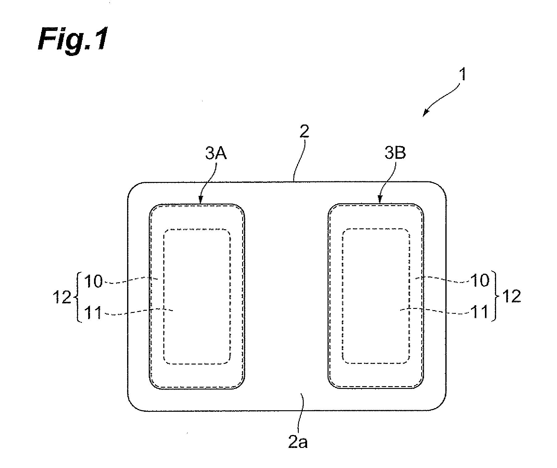
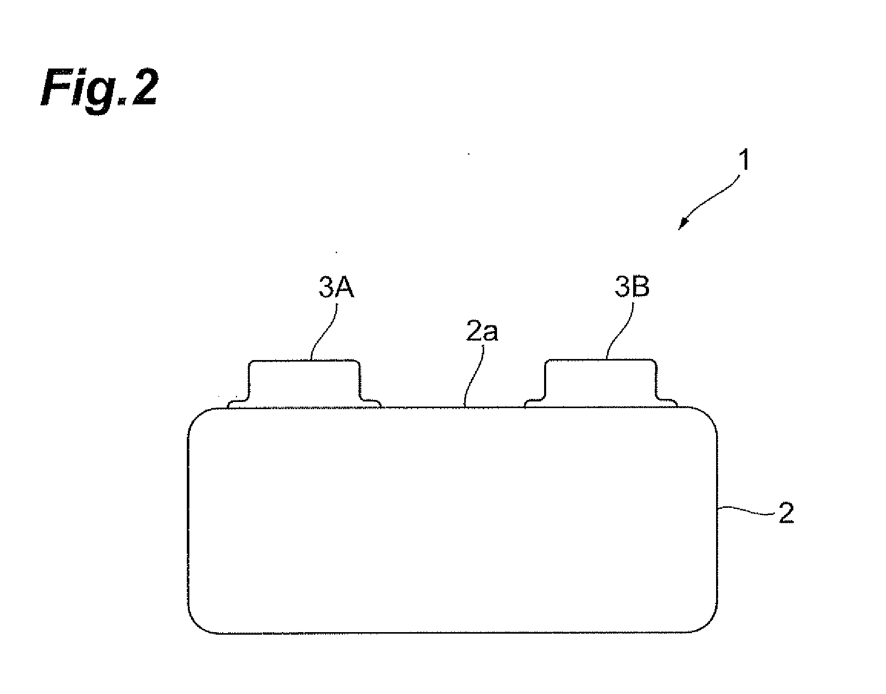
[0021]FIG. 1 is a plan view showing a chip varistor as an embodiment of the electronic component according to the present invention and FIG. 2 a side view of the chip varistor shown in FIG. 1. In each drawing, the chip varistor 1 is a flip chip varistor of a bottom electrode type.

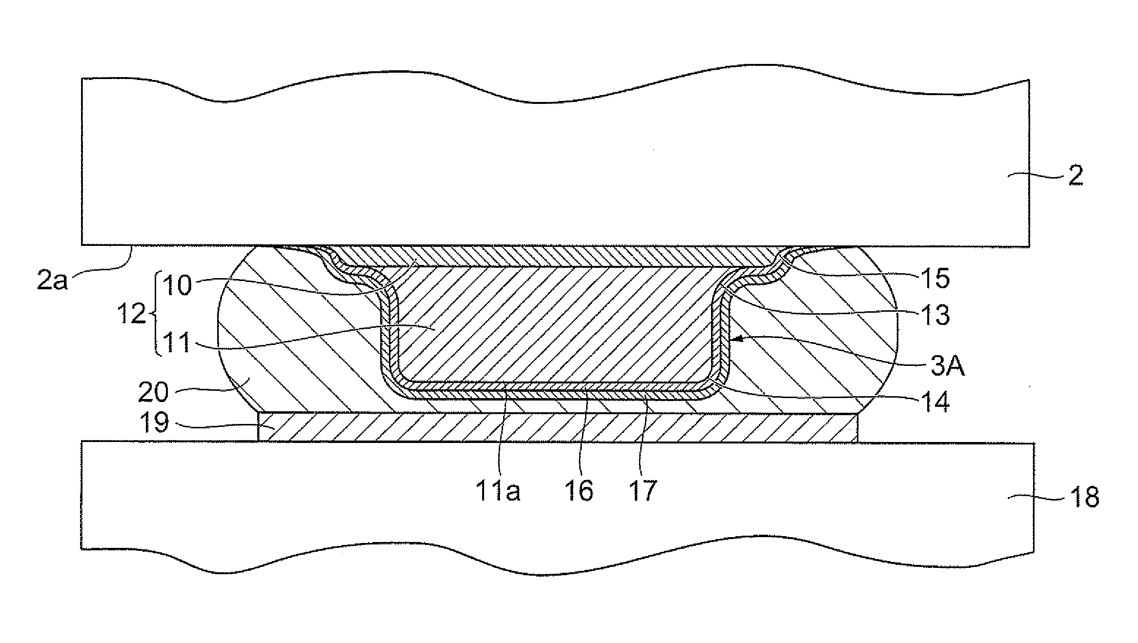
[0022]The chip varistor 1 has a chip element body 2 of a nearly rectangular parallelepiped shape, and external electrodes 3A, 3B formed on one principal surface 2a of this chip element body 2. The size of the chip element body 2 is, for example, approximately 0.5 mm×0.7 mm×0.3 mm.

[0023]The chip element body 2, as shown in FIG. 3, is a laminate in which varistor layer 4 to exhibit the nonlinear voltage-current characterist...


PUM


Abstract

An electronic component has an element body, and a plurality of external electrodes formed on one principal face of the element body. Each external electrode has a first electrode layer joined to the one principal face of the element body, and a second electrode layer joined as laid on an inside region inside an edge of the first electrode layer. An apical surface of the second electrode layer is planar. A joint portion in the second electrode layer to the first electrode layer is rounded.

Description

BACKGROUND OF THE INVENTION[0001]1. Field of the Invention[0002]The present invention relates to an electronic component with external electrodes on one principal face of an element body.[0003]2. Related Background Art[0004]There is a known conventional electronic component in which a plurality of connection pads are formed on a lower face of a chip body and in which a gold bump is formed through an underlying metal layer under an exposed surface of each connection pad, for example, as described in Japanese Patent Application Laid-open No. 10-12668).SUMMARY OF THE INVENTION[0005]However, the foregoing conventional technology has the following problem. Namely, if solder is used to join the gold bumps to corresponding gold bumps on a circuit board in order to simply and inexpensively mount the electronic component on the circuit board, the solder can fail to fully wrap around a joint portion of each gold bump, so as to result in insufficient adhesion strength between the electronic co...

Claims


Application Information

Patent Timeline
Patent Type & Authority Applications(United States)
IPC IPC(8): H05K1/11
CPCH01G2/06H05K3/3436H01G4/005
Inventor MURAKAMI, YUKIHIROSATOH, YOSHIHIKOMORIAI, KATSUNARITAKEYA, KAZUTOKURIMOTO, SATOSHI
Owner TDK CORPARATION
Why Eureka
Try Eureka