METAL GATE STRESS FILM FOR MOBILITY ENHANCEMENT IN FinFET DEVICE

a technology of metal gate stress film and finfet device, which is applied in the direction of semiconductor device, transistor, electrical apparatus, etc., can solve the problem that known stressors such as nitride cap are not applicable to highly integrated finfet devi

Inactive Publication Date: 2010-03-25
TAIWAN SEMICON MFG CO LTD
View PDF19 Cites 159 Cited by
  • Summary
  • Abstract
  • Description
  • Claims
  • Application Information

AI Technical Summary

Problems solved by technology

Furthermore, known stressors such as nitride-caps are not applicable to highly integrated FinFET devices which may include fins that are spaced apart by as little as 25 nm, such spacings producing trenches with high aspect ratios, and also due to increased parasitic capacitance issues stemming from the high-dielectric constant of the nitride film.

Method used


Image

  • METAL GATE STRESS FILM FOR MOBILITY ENHANCEMENT IN FinFET DEVICE
  • METAL GATE STRESS FILM FOR MOBILITY ENHANCEMENT IN FinFET DEVICE
  • METAL GATE STRESS FILM FOR MOBILITY ENHANCEMENT IN FinFET DEVICE

Examples


Embodiment Construction

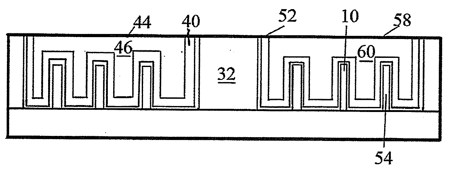
[0019]The present invention provides a sequence of process operations that effectively generates compressive and tensile stresses on NMOS and PMOS FinFET devices, respectively, by manipulating mechanical properties, in particular the stress characteristics, of thin metal gates to enhance both electron and hole mobility. The methods and structure of the invention can be used on planar devices or FinFET devices formed on closely spaced fins, i.e., fins with high aspect ratios that are spaced apart by about 25 nm or less, and can be understood according to the following illustrated exemplary sequence of processing operations carried out to produce FinFET devices.

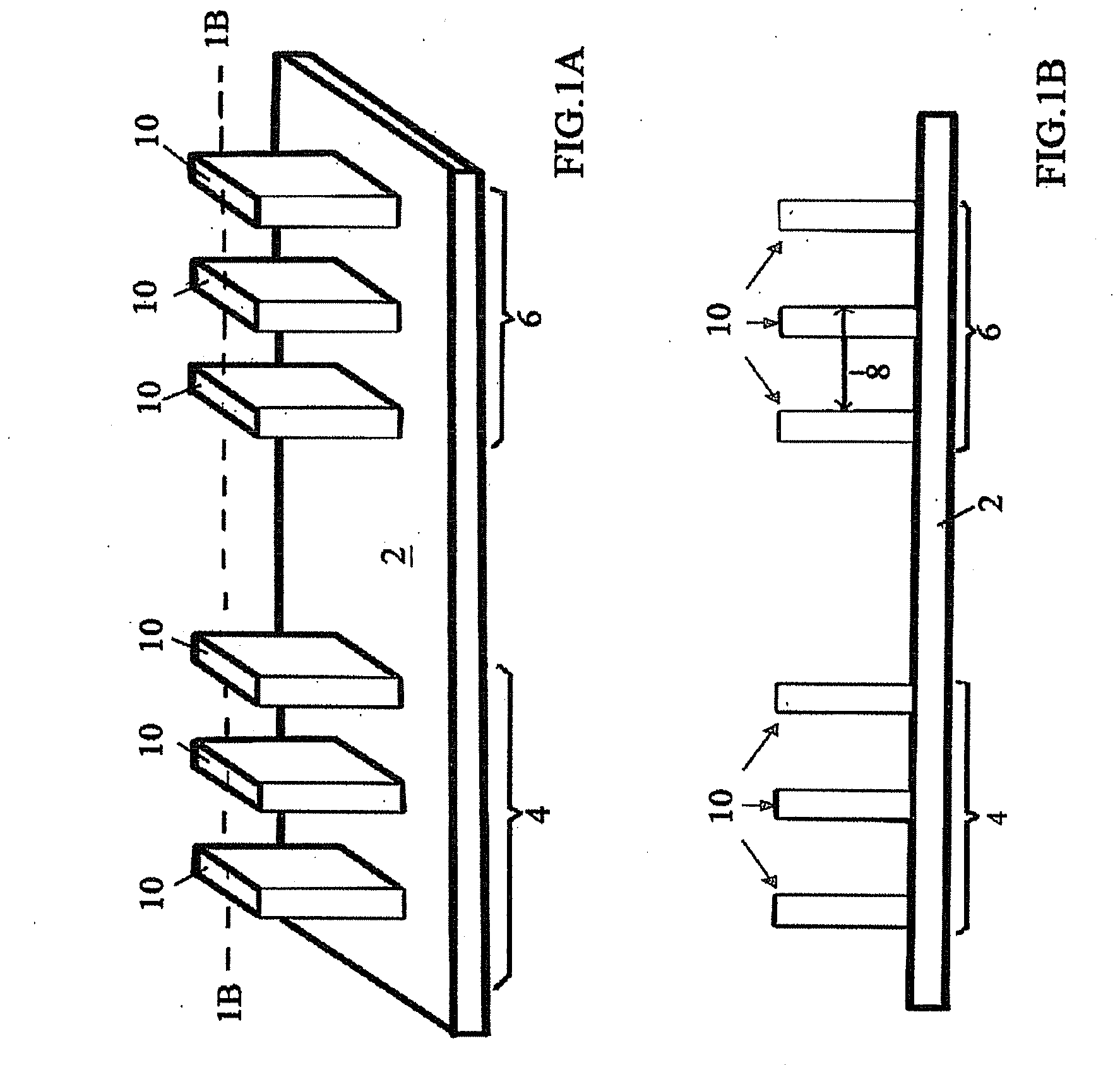
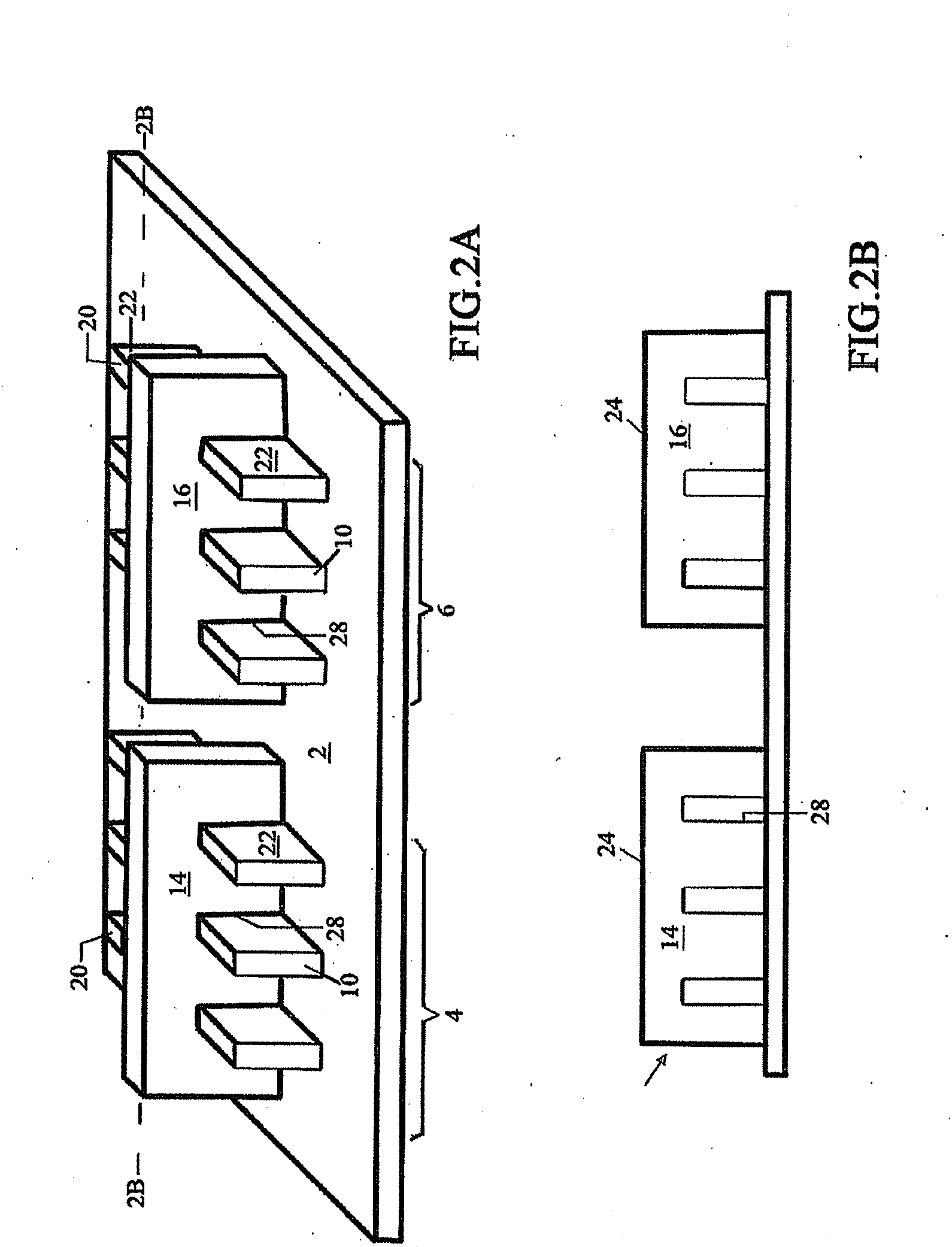
[0020]FIGS. 1A, 1B show substrate 2 having PMOS region 4 and NMOS region 6. In each of PMOS region 4 and NMOS region 6 are fins 10. Fins 10 may be formed of silicon, silicon-germanium (SiGe), Ge, various group III-IV compound semiconductors or other suitable semiconductor materials used for fins in FinFET devices. Fins 10 may i...


PUM

PropertyMeasurementUnit
tensile stressaaaaaaaaaa
thicknessaaaaaaaaaa
thicknessaaaaaaaaaa

Abstract

A CMOS FinFET semiconductor device provides an NMOS FinFET device that includes a compressive stress metal gate layer over semiconductor fins and a PMOS FinFET device that includes a tensile stress metal gate layer over semiconductor fins. A process for forming the same includes a selective annealing process that selectively converts a compressive metal gate film formed over the PMOS device to the tensile stress metal gate film.

Description

FIELD OF THE INVENTION[0001]The present invention relates, most generally, to semiconductor devices and methods for manufacturing the same. More particularly, the present invention relates to FinFET logic devices, other CMOS devices and methods for manufacturing the same.BACKGROUND[0002]In the rapidly advancing semiconductor manufacturing industry, CMOS, complimentary metal oxide semiconductor, FinFET devices are favored for many logic and other applications and are integrated into various different types of semiconductor devices. FinFET devices typically include semiconductor fins with high aspect ratios and in which channel and source / drain regions of semiconductor transistor devices are formed. A gate is formed over and along the sides of the fin devices utilizing the advantage of the increased surface area of the channel and source / drain regions to produce faster, more reliable and better-controlled semiconductor transistor devices.[0003]In FinFET and conventional planar transis...

Claims


Application Information

Patent Timeline
Patent Type & Authority Applications(United States)
IPC IPC(8): H01L21/8238H01L27/092
CPCH01L21/823807H01L21/823821H01L21/823828H01L29/785H01L29/66545H01L29/66795H01L21/845
Inventor XU, JEFF J.WANN, CLEMENT H.YEH, CHIH CHIEHCHANG, CHIH-SHENG
Owner TAIWAN SEMICON MFG CO LTD
Why Eureka
Try Eureka