
Method for transferring chips onto a substrate

Inactive Publication Date: 2010-03-25
COMMISSARIAT A LENERGIE ATOMIQUE ET AUX ENERGIES ALTERNATIVES
View PDF15 Cites 9 Cited by
  • Summary
  • Abstract
  • Description
  • Claims
  • Application Information

AI Technical Summary

Benefits of technology

[0027]The thermal budget for step b) can increase the weakening induced by implantation, corresponding to about 85% or 90% of the total thermal budget necessary to obtain the fracture along the weakened zone.

Problems solved by technology

The wafer-to-wafer transfer is technologically simpler, but it is subject to serious limitations:chips for boards to be transferred must be the same size, and this creates a very strong constraint on the design, practically making it impossible to purchase boards from different suppliers to assemble them,the efficiency of transferred chips quickly makes this technique unacceptable; for example for the case of chips with an efficiency of 85% (mature system), an operation to transfer 5 boards on top of each other will result in a final total efficiency of only 44%.
The technique for transferring chips onto a wafer offers another solution, but it must use increasingly thin chips which creates other problems.
Its major disadvantage is due to the fact that the handle of each chip has to be separated individually; for example, if 1×1 cm2 chips are transferred at a pitch of 1.5 cm onto a 300 mm diameter wafer, about 310 chips have to be separated individually per wafer, which is unacceptable,“resin” type bonding, with disassembly of the temporary handle by heat treatment, often mechanically assisted (shear).
The difficulties are both due to the individual mechanical action and management of bonding resin residues.
Furthermore, the grinding technique used to thin boards, which in the best case introduces a thickness variation of + / −1 μm for thinning leading to thinned chip thicknesses of up to 5-10 μm, which is still not sufficient.
Such a thickness variation requires super-etching of vias which limits the density and increases the cost, and limits the production and precision of subsequent planarising.
Therefore, the problem that arises is to find a new method by which components can be transferred onto a wafer, particularly in order to stack component stages.

Method used


Image

  • Method for transferring chips onto a substrate
  • Method for transferring chips onto a substrate
  • Method for transferring chips onto a substrate

Examples


Embodiment Construction

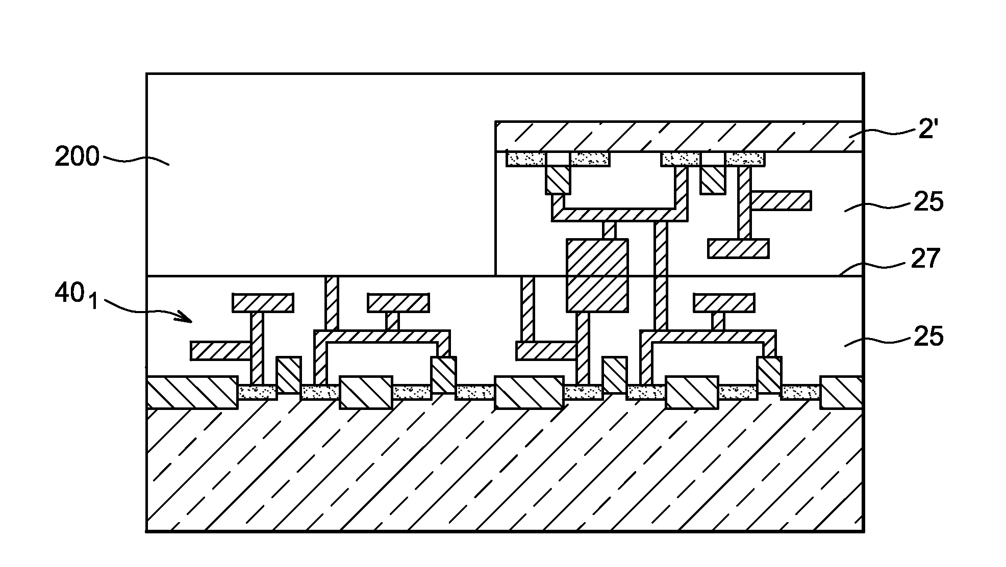
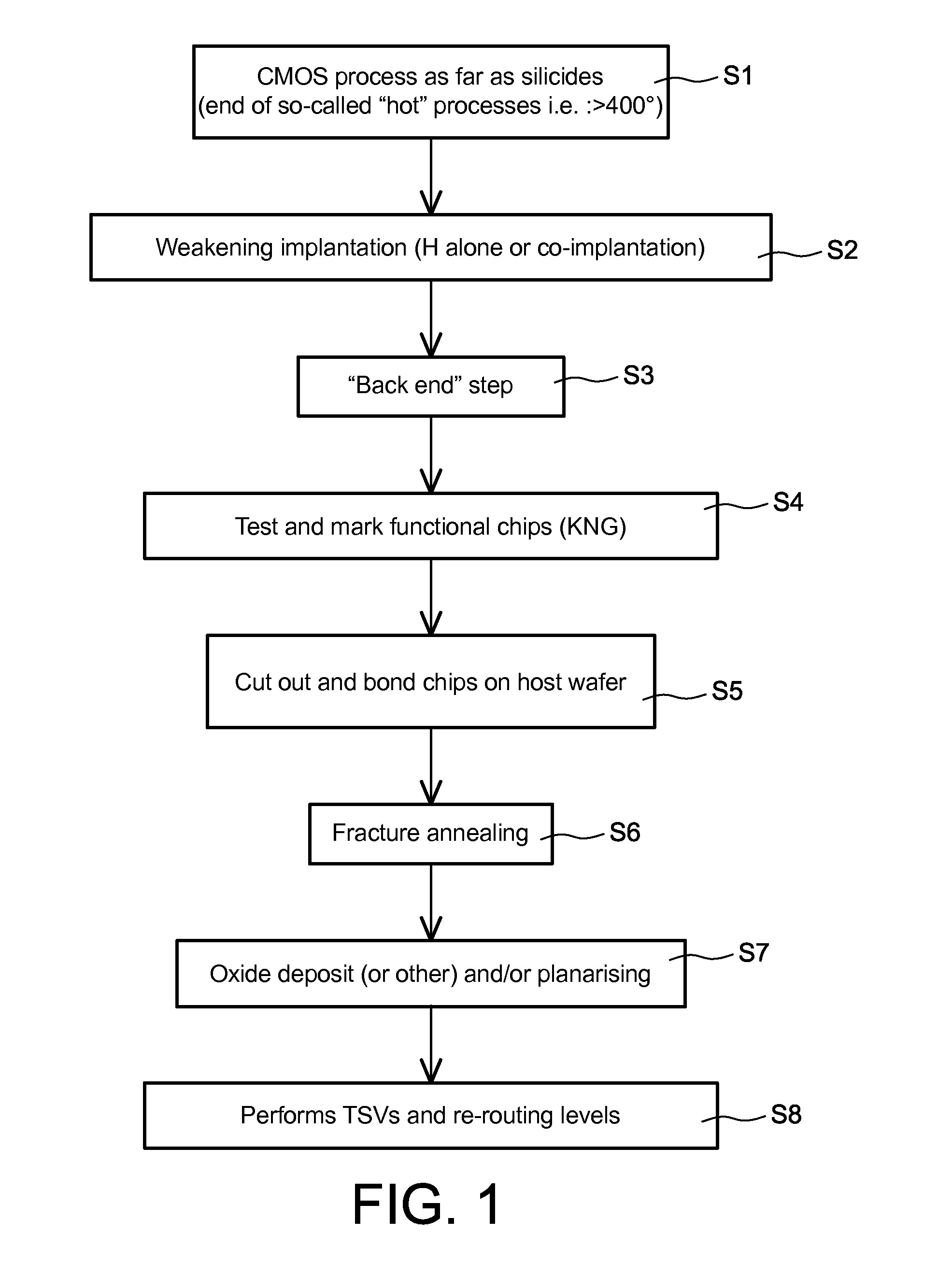
[0040]FIG. 1 shows the steps in a method according to the invention.

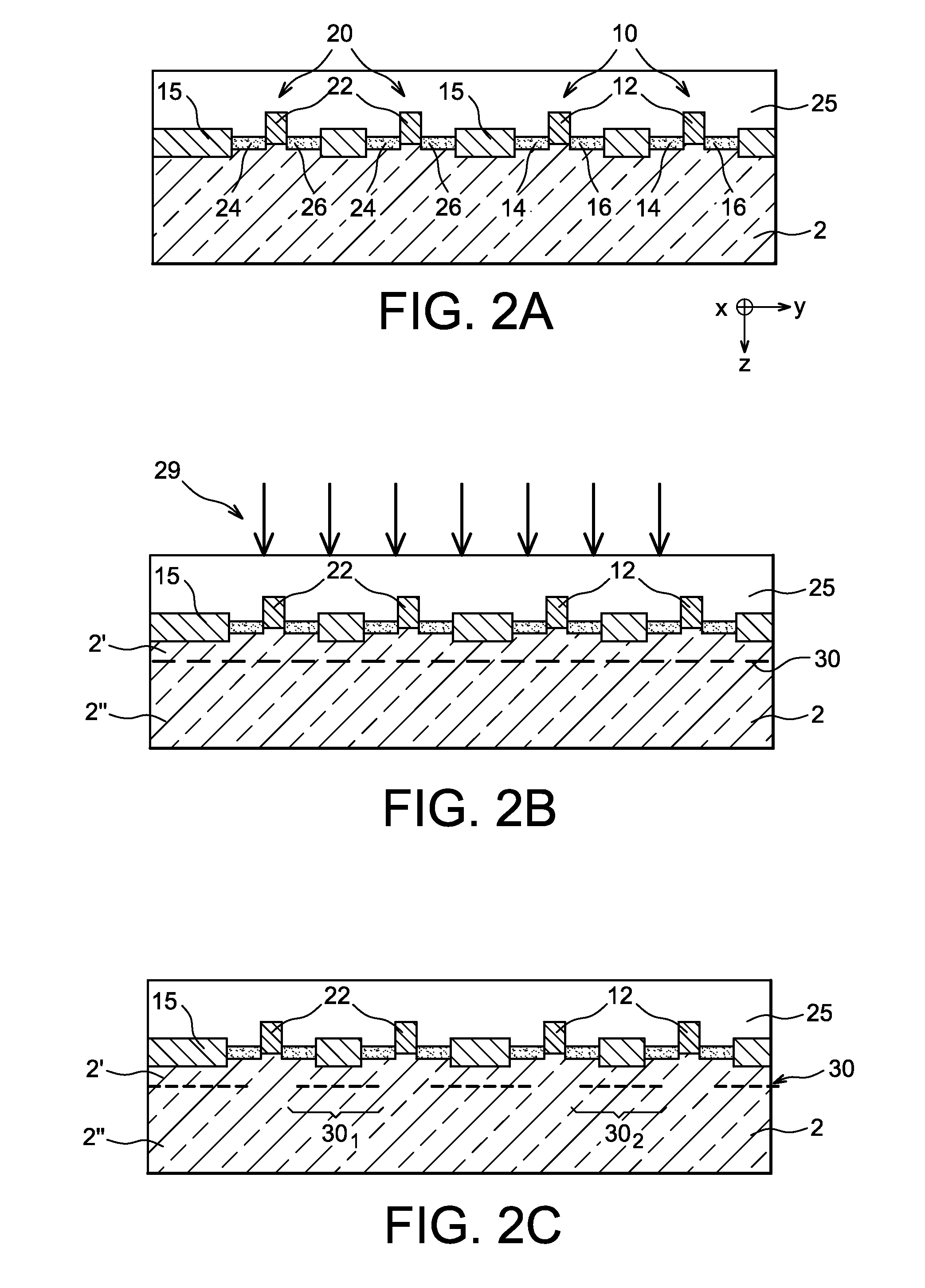
[0041]Each of these steps is shown in a more detailed manner within the framework of a simple example, the chaining in FIGS. 2A-2H. This example in FIGS. 2A-2H will be described in parallel with FIG. 1 and is deliberately simplified to facilitate understanding.

[0042]This description relates to the production of CMOS components.

[0043]In a first step (S1), a plurality of CMOS components 10, 20 each comprising a gate 12, 22, a drain and a source made by doping is made in or on a substrate 2 made of a semiconducting material, for example silicon, and a drain silicide 14, 24 and a source silicide 16, 26 respectively are then formed on top of said drain and said source (FIG. 2A). For example, each of these silicides is made from a Pt, or Pd, or Ni, or Co, or Ti silicide, . . . FIG. 2A also shows transistor isolation oxides 15 (STI oxide). A dielectric 25 (called PMD or “Pre Metal Deposition”) is formed and is planarised o...


PUM


Abstract

The invention relates to a method for making a stack of at least two stages of circuits, each stage comprising a substrate and at least one component (10, 20) and metallic connections formed in or on this substrate, the assembly of a stage to be transferred onto a previous stage comprising:a) ionic implantation (29) in the substrate (2, 25) of the stage to be transferred through at least part of the components (10, 20), so as to form a weakened zone (30),b) formation of metallic connections of said components,c) transfer and assembly of some of this substrate onto the previous stage,d) a step to thin the transferred part of said substrate by fracture along the weakened zone (30).

Description

TECHNICAL FIELD AND PRIOR ART[0001]The invention relates to the field of stacking semiconductor circuits and techniques for making such stacks, and particularly techniques for transferring components or chips made of semiconducting materials onto a wafer.[0002]Circuits are stacked by two types of techniques at the present time, namely techniques for making transfers from wafer-to-wafer and techniques for transferring chips onto boards.[0003]The wafer-to-wafer transfer is technologically simpler, but it is subject to serious limitations:[0004]chips for boards to be transferred must be the same size, and this creates a very strong constraint on the design, practically making it impossible to purchase boards from different suppliers to assemble them,[0005]the efficiency of transferred chips quickly makes this technique unacceptable; for example for the case of chips with an efficiency of 85% (mature system), an operation to transfer 5 boards on top of each other will result in a final ...

Claims


Application Information

Patent Timeline
IPC IPC(8): H01L21/50
CPCH01L21/7813H01L25/0657H01L25/50H01L2225/06513H01L2924/0002H01L2225/06541H01L2924/00H01L24/80H01L2224/08145H01L21/2007
Inventor CLAVELIER, LAURENTDEGUET, CHRYSTELLEDUC, PATRICKMORICEAU, HUBERT
Owner COMMISSARIAT A LENERGIE ATOMIQUE ET AUX ENERGIES ALTERNATIVES
Learn More