Semiconductor device

Inactive Publication Date: 2010-04-01
ROHM CO LTD
View PDF2 Cites 0 Cited by
  • Summary
  • Abstract
  • Description
  • Claims
  • Application Information

AI Technical Summary

Benefits of technology

[0026]The semiconductor device may further include a barrier metal interposed between the interlayer insulating film and

Problems solved by technology

However, with this method, once the AlCu alloy film is formed, it is extremely difficult to align (position) a mask in a photolithography process for patterning the AlCu al

Method used


Image

  • Semiconductor device
  • Semiconductor device
  • Semiconductor device

Examples


Embodiment Construction

)

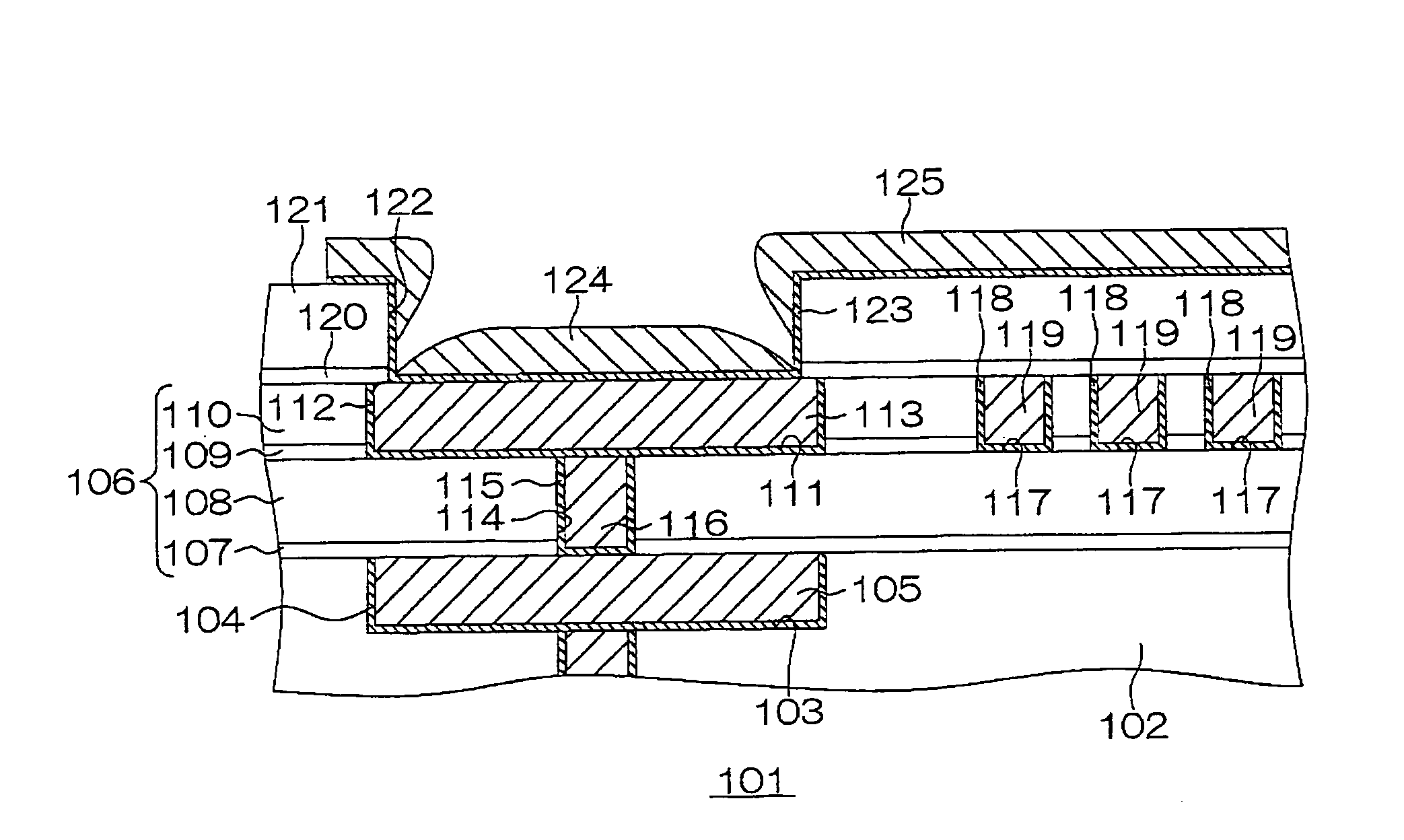
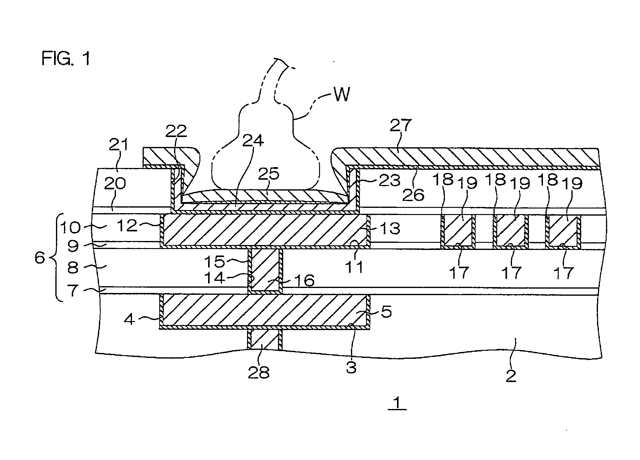
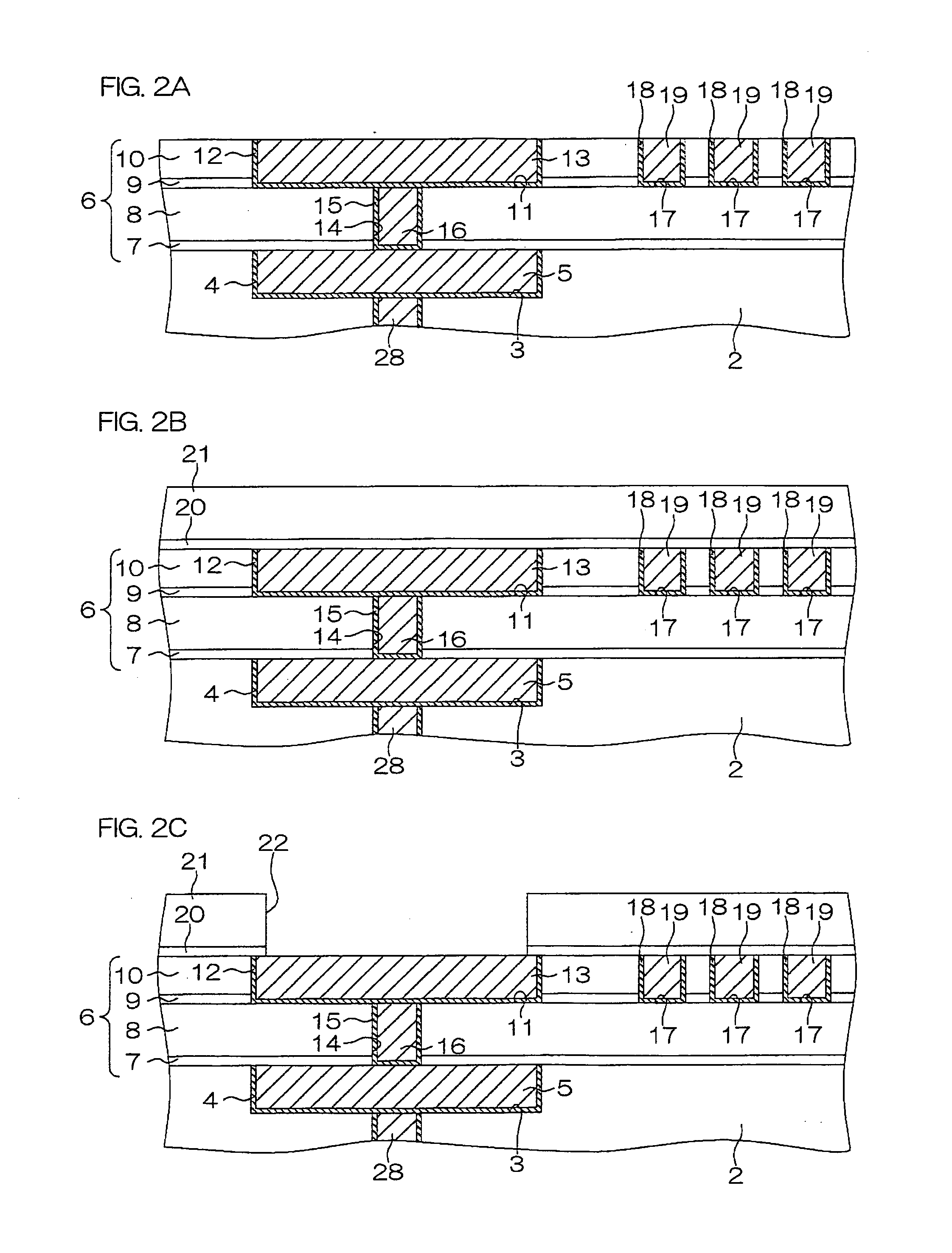
[0033]FIG. 1 is a schematic sectional view of a semiconductor device according to an embodiment of the present invention.

[0034]The semiconductor device 1 is a transformer device and includes an unillustrated semiconductor substrate. An Si (silicon) substrate, an SiC (silicon carbide) substrate, etc., can be cited as examples of the semiconductor substrate.

[0035]A first insulating layer 2 is laminated on the semiconductor substrate. The first insulating layer 2 is made, for example, of SiO2.

[0036]A first wiring groove 3 is formed in the first insulating layer 2. The first wiring groove 3 has a recessed form formed by digging in from an upper surface of the first insulating layer 2.

[0037]A barrier metal 4 is formed on inner surfaces (a side surface and a bottom surface) of the first wiring groove 3. The barrier metal 4 has a structure where, for example, a Ta (tantalum) film, a TaN (tantalum nitride) film, and a Ta film are laminated in that order from the bottom. Then, a first wirin...


PUM


Abstract

A semiconductor device according to the present invention includes: a wiring; an interlayer insulating film formed over the wiring and having an opening reaching the wiring from a top surface thereof; an intra-opening metal film formed on the wiring inside the opening and made of a metal material that contains aluminum; a top surface metal film formed over the interlayer insulating film and made of the metal material; and a conduction securing film formed on a side surface of the opening to secure conduction between the intra-opening metal film and top surface metal film.

Description

BACKGROUND OF THE INVENTION[0001]1. Field of the Invention[0002]The present invention relates to a semiconductor device and particularly to a power semiconductor device.[0003]2. Description of the Related Art[0004]Recently, in the field of power electronics, power semiconductor devices that include a transformer (hereinafter referred to as “transformer devices”) have been developed.[0005]FIG. 3 is a schematic sectional view of a transformer device.[0006]The transformer device 101 includes a first insulating layer 102 made of SiO2 (silicon oxide) on a semiconductor substrate not shown.[0007]A first wiring groove 103 is formed in the first insulating layer 102. A first wiring 105, formed of a metal material having Cu (copper) as a main component (hereinafter referred to as the “Cu wiring material”), is embedded via a barrier metal 104 in the first wiring layer 103.[0008]A second insulating layer 106 is laminated on the first insulating layer 102. The second insulating layer 106 has a ...

Claims


Application Information

Patent Timeline
IPC IPC(8): H01L23/52H01L23/552
CPCH01L23/5225H01L23/5227H01L2924/0002H01L2224/05556H01L2924/01033H01L2924/01006H01L2924/3025H01L2924/05042H01L2924/04953H01L2924/01074H01L2924/01073H01L2924/0105H01L2924/01029H01L2924/01022H01L2924/01014H01L23/53238H01L23/53295H01L23/552H01L23/645H01L24/03H01L24/05H01L24/48H01L2224/04042H01L2224/05006H01L2224/05084H01L2224/05166H01L2224/05181H01L2224/05187H01L2224/05572H01L2224/05624H01L2224/05647H01L2224/48463H01L2924/01004H01L2924/01013H01L2924/00014H01L2924/04941H01L2224/05552H01L2224/05093H01L2224/45099
Inventor NAKAO, YUICHINAKAGAWA, RYOSUKE
Owner ROHM CO LTD
Why Eureka
Try Eureka