Semiconductor device

Inactive Publication Date: 2005-11-24
KK TOSHIBA
View PDF6 Cites 2 Cited by
  • Summary
  • Abstract
  • Description
  • Claims
  • Application Information

AI Technical Summary

Benefits of technology

[0010] According to an aspect of the present invention, there is provided a semiconductor device comprising: a semiconductor substrate; an insulating region provided on the semiconductor substrate; a first capacitor provided above the insulating region; a second capacitor provided above the insulating region and adjacent to the first capacitor; a conductive hydrogen-bar

Problems solved by technology

In such cases, it is difficult to obtain an opti

Method used


Image

  • Semiconductor device
  • Semiconductor device
  • Semiconductor device

Examples


Example

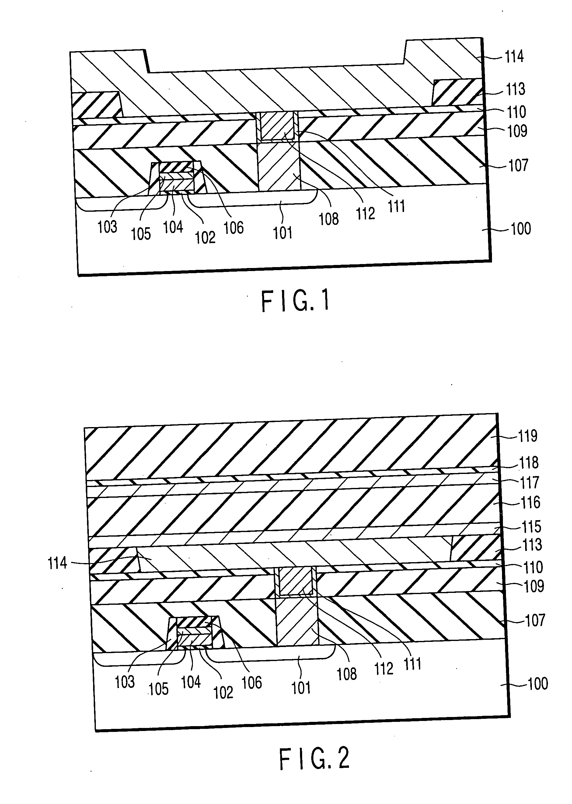
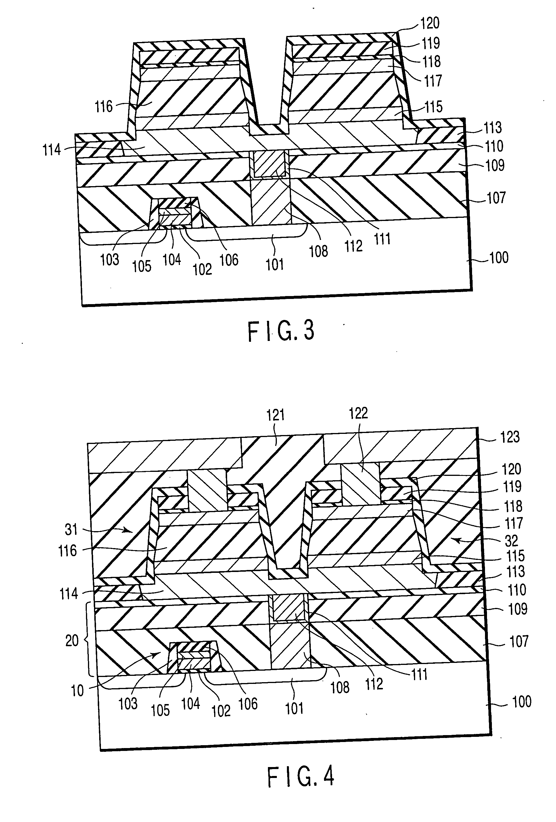
[0015] An embodiment of the present invention is explained below with reference to drawings. FIGS. 1 to 4 are schematic cross-sectional views of manufacturing steps of a semiconductor device according to the embodiment of the present invention.

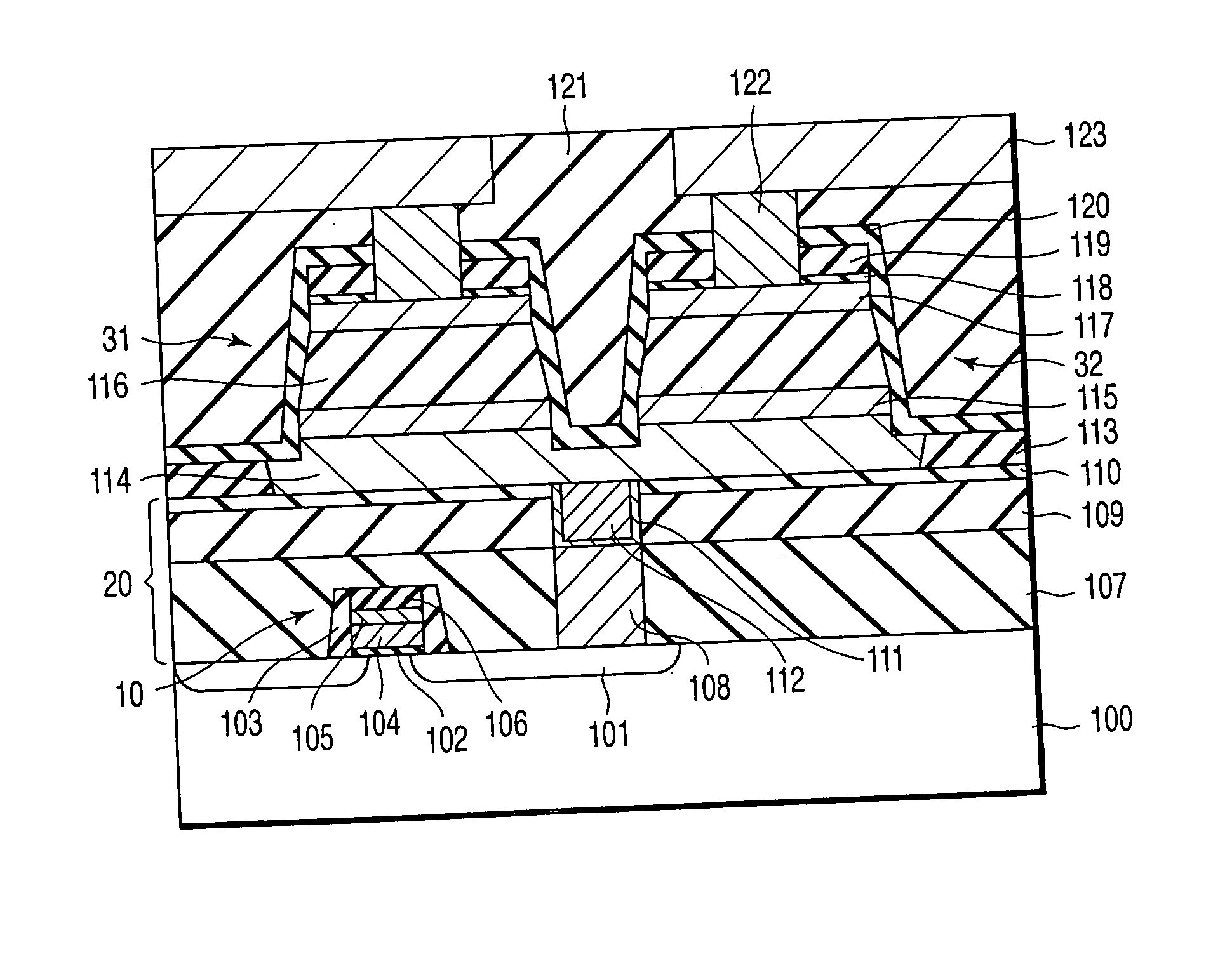
[0016] First, a structure of a semiconductor device (ferroelectric memory) according to the embodiment of the present invention is explained with reference to FIG. 4.

[0017] An isolating region (not shown) and a MIS transistor 10 are formed in a surface region of a p type silicon substrate (semiconductor substrate) 100. The MIS transistor 10 comprises a gate insulating film 102, a gate electrode (word line) formed of a polysilicon film 104 and a tungsten silicide film 105, a gate cap film 106, gate side wall films 103, and source / drain diffusion layers 101.

[0018] On the silicon substrate 100, formed is an insulating region 20 which includes an interlayer insulating film 107, a polysilicon plug 108, an interlayer insulating film 109, an inter...


PUM


Abstract

Disclosed is a semiconductor device comprising a semiconductor substrate, an insulating region provided on the semiconductor substrate, a first capacitor provided above the insulating region, a second capacitor provided above the insulating region and adjacent to the first capacitor, a conductive hydrogen-barrier film which prevents diffusion of hydrogen into the first and second capacitors and connects a bottom electrode of the first capacitor with a bottom electrode of the second capacitor, the conductive hydrogen-barrier film having a first portion interposing between the insulating region and the first capacitor and between the insulating region and the second capacitor.

Description

CROSS-REFERENCE TO RELATED APPLICATIONS [0001] This application is based upon and claims the benefit of priority from prior Japanese Patent Application No. 2004-147725, filed May 18, 2004, the entire contents of which are incorporated herein by reference. BACKGROUND OF THE INVENTION [0002] 1. Field of the Invention [0003] This invention relates to a semiconductor device having a capacitor. [0004] 2. Description of the Related Art [0005] Recently, ferroelectric memories in which a ferroelectric film is used as a dielectric film of a capacitor, that is, FeRAMs (Ferroelectric Random Access Memory) have been developed. [0006] In manufacture of ferroelectric capacitors, various processing in a reducing atmosphere is performed, such as processing a capacitor by RIE (reactive ion etching), deposition of an interlayer insulating film by CVD (chemical vapor deposition), and formation of a contact hole by RIE. Therefore, to prevent reduction of the capacitor insulating film (dielectric film),...

Claims


Application Information

Patent Timeline
IPC IPC(8): H01L21/02H01L27/105H01L21/8246H01L27/115H01L29/94
CPCH01L27/11502H01L28/65H01L28/57H01L27/11507H10B53/00H10B53/30
Inventor YAMAZAKI, SOICHIYAMAKAWA, KOJI
Owner KK TOSHIBA
Why Eureka
Try Eureka