BiSb Topological Insulator with Seed Layer or Interlayer to Prevent Sb Diffusion and Promote BiSb (012) Orientation

Active Publication Date: 2021-10-28
WESTERN DIGITAL TECH INC
View PDF0 Cites 4 Cited by
  • Summary
  • Abstract
  • Description
  • Claims
  • Application Information

AI Technical Summary

Benefits of technology

The patent is about a new type of material called bismuth antimony (BiSb) topological insulator, which can prevent the diffusion of antimony and promote better orientation of the material. This material is important for making a spin-orbit torque (SOT) magnetic tunnel junction (MTJ) device. The patent describes several methods for improving the performance of the device by using different layers and materials, such as a seed layer, an interlayer, or an amorphous film. These improvements can lead to higher efficiency, better accuracy, and more reliable functionality of the SOT MTJ device.

Problems solved by technology

However, BiSb materials have not yet been adopted in commercial SOT applications due to several obstacles.
For example, BiSb materials are generally soft, have low melting points, have large grain sizes, are easily damaged by ion milling, have significant Sb migration issues upon thermal annealing due to its film roughness, and have difficulty maintaining a (012) orientation for maximum spin Hall effect.

Method used


Image

  • BiSb Topological Insulator with Seed Layer or Interlayer to Prevent Sb Diffusion and Promote BiSb (012) Orientation
  • BiSb Topological Insulator with Seed Layer or Interlayer to Prevent Sb Diffusion and Promote BiSb (012) Orientation
  • BiSb Topological Insulator with Seed Layer or Interlayer to Prevent Sb Diffusion and Promote BiSb (012) Orientation

Examples


examples

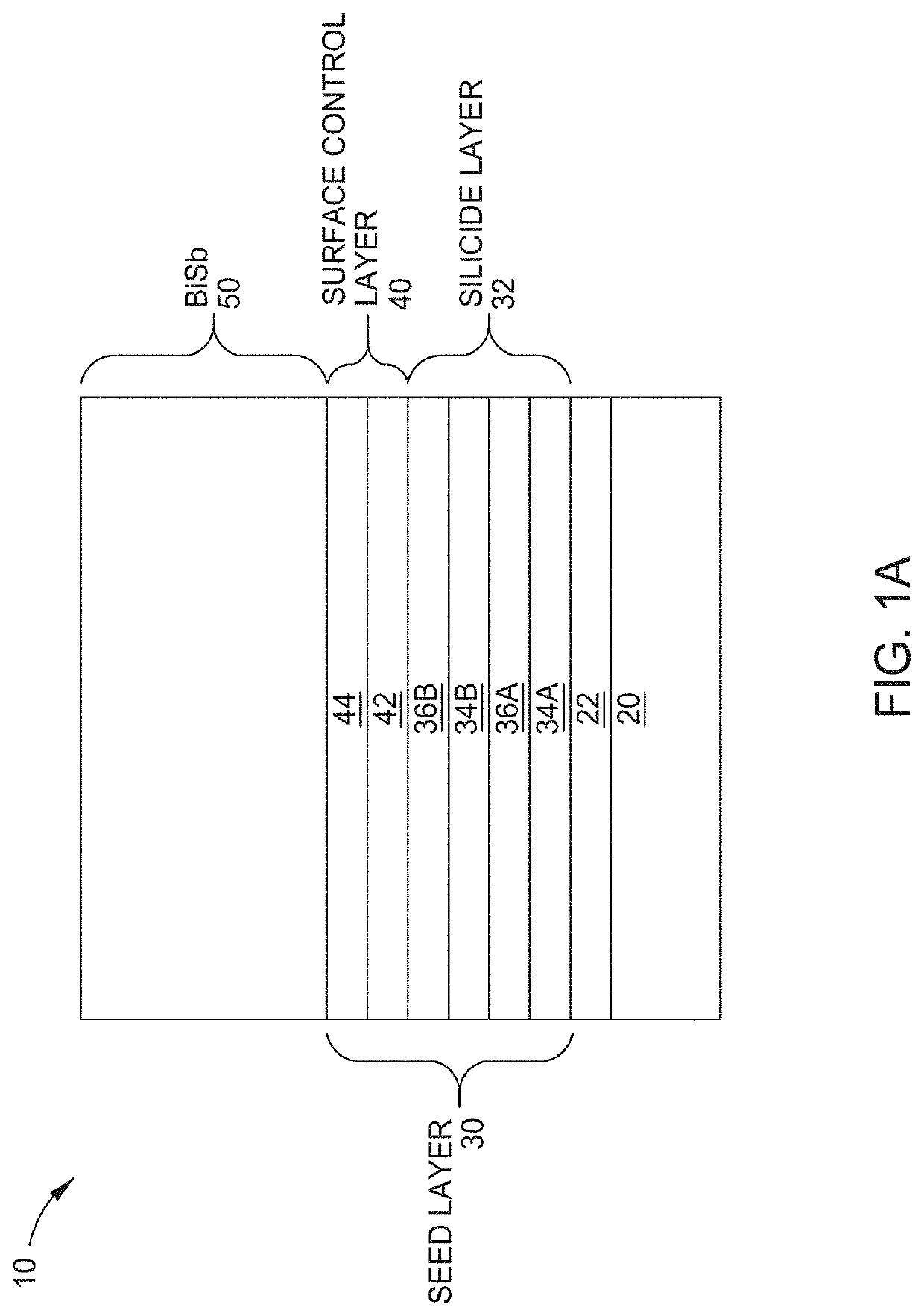
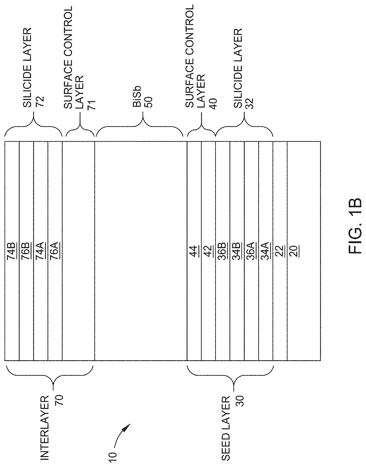
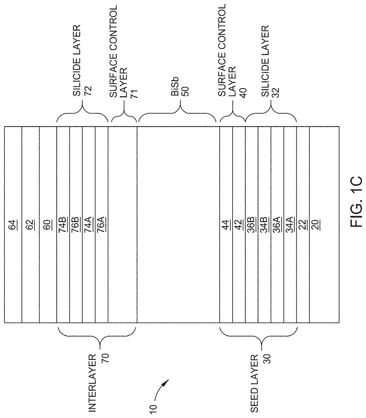
[0076]The following are examples to illustrate various embodiments of a BiSb layer, such as the BiSb layer 50 of FIGS. 1A-1E, the magnetic drive 100 of FIG. 3, the write head 210 of FIG. 3, the SOT MTJ devices 230 of FIGS. 4 and 5, other BiSb layers, other magnetic drives, other SOT MTJ devices, and variations thereof. These examples are not meant to limit the scope of the claims unless specifically recited in the claims.

example a

[0077]In Example A, a sample was formed by physical vapor deposition (PVD) of a base layer of non-conductive amorphous silicon to a thickness of about 18 Å. A single composition graded silicide layer was formed by PVD on the base layer of a laminate Si / NiFe stack with the approximate thicknesses of Si 4 Å, NiFe 2 Å, Si 4 Å, NiFe 2 Å, Si 4 Å, and NiFe 5 Å. A surface control layer of Cu was formed by PVD on the NiFe 5 Å layer to a thickness of about 5 Å silicide layer deposited by PVD. The surface control layer was made of Cu 5 Å. A BiSb layer was formed by PVD on the Cu layer to a thickness of about 100 Å. X-ray diffraction (XRD) 2Θ scans of the sample was conducted as shown in FIG. 6. The BiSb layer showed (012) orientation with a low or no amount of (003) orientation.

example b

[0078]In Example B, sample 710 was formed by PVD of a laminate stack with the approximate thicknesses of Si 14 Å and a NiFe 7 Å. The laminate stack formed a high-resistance, single-composition, graded, silicide layer after room temperature intermixing. A surface control layer of Cu was formed by PVD on the silicide layer to a thickness of about 5 Å. A BiSb layer was formed by PVD on the surface control layer to a thickness of about 100 Å. An interlayer of a laminate stack with the approximate thicknesses of Si 10 Å, NiFe 5 Å, Si 10 Å, and NiFe 5 Å was formed by PVD on the BiSb layer. The interlayer laminate stack formed a high-resistance, single-composition, graded, silicide layer after room temperature intermixing.

[0079]Sample 720 was formed by PVD of a seed layer of a laminate stack with the approximate thickness of Si 16 Å and a NiFe 7 Å. The seed layer laminate stack formed a high-resistance, single-composition, graded, silicide layer after room temperature intermixing. A surfac...


PUM


Abstract

A spin-orbit torque (SOT) magnetic tunnel junction (MTJ) device includes a substrate, a seed layer over the substrate, and a bismuth antimony (BiSb) layer having (0120) orientation on the seed layer. The seed layer includes a silicide layer and a surface control layer. The silicide layer includes a material of NiSi, NiFeSi, NiFeTaSi, NiCuSi, CoSi, CoFeSi, CoFeTaSi, CoCuSi, or combinations thereof. The surface control layer includes a material of NiFe, NiFeTa, NiTa, NiW, NiFeW, NiCu, NiCuM, NiFeCu, CoTa, CoFeTa, NiCoTa, Co, CoM, CoNiM, CoNi, NiSi, CoSi, NiCoSi, Cu, CuAgM, CuM, or combinations thereof, in which M is Fe, Cu, Co, Ta, Ag, Ni, Mn, Cr, V, Ti, or Si.

Description

BACKGROUND OF THE DISCLOSUREField of the Disclosure[0001]Embodiments of the present disclosure generally relate to a bismuth antimony (BiSb) topological insulator with a seed layer and / or an interlayer to prevent Sb diffusion and to promote BiSb (012) orientation.Description of the Related Art[0002]BiSb with (012) orientation is a narrow gap topological insulator with both giant spin Hall effect and high electrical conductivity. BiSb is a material that has been proposed in various spin-orbit torque (SOT) magnetic tunnel junction (MTJ) applications, such as for a spin Hall layer for energy-assisted magnetic recording write heads and magnetoresistive random access memory (MRAM) devices.[0003]However, BiSb materials have not yet been adopted in commercial SOT applications due to several obstacles. For example, BiSb materials are generally soft, have low melting points, have large grain sizes, are easily damaged by ion milling, have significant Sb migration issues upon thermal annealing...

Claims


Application Information

Patent Timeline
IPC IPC(8): H01L43/04H01L27/22H01L43/06H01L43/10H01F10/32G11B5/39
CPCH01L43/04H01L27/222H01L43/06G11B2005/0018H01F10/3254H01F10/3272G11B5/3909H01L43/10G11B2005/0032G11B2005/0024G11B5/3133H01F10/30H01F10/329B82Y25/00H10B61/00H10N50/80H10N50/01H10N50/10H10N52/80H10N50/85H10N52/00
Inventor LE, QUANGHWANG, CHERNGYEYORK, BRIAN R.CHEN, ANDREWNGUYEN, THAO A.AHN, YONGCHULLIU, XIAOYONGJIANG, HONGQUANGAO, ZHENGHO, KUOK SAN
Owner WESTERN DIGITAL TECH INC
Why Eureka
Try Eureka