Semiconductor device and method of manufacturing the same

Active Publication Date: 2006-09-28
RENESAS ELECTRONICS CORP
View PDF4 Cites 0 Cited by
  • Summary
  • Abstract
  • Description
  • Claims
  • Application Information

AI Technical Summary

Benefits of technology

[0012] Accordingly, an object of the invention is to provide a semiconductor device having a gate electrode stable that can stably maintain a desired work function even when it is subjected to heat treatment, and to provide a method of manufacturing the same.
[0013] For achieving the above object, the semiconductor device according to the invention includes a semiconductor substrate, a gate insulating film formed in contact with an upper side of the semiconductor substrate, and a gate electrode made of metal nitride or metal nitride silicide and formed on the upper side of the gate insulating film. A buffer layer preventing diffusion of the nitrogen and silicon is interposed between the gate insulating film and the gate electrode.

Problems solved by technology

When the titanium nitride already described is used in the process of manufacturing the conventional CMOS structure, such a problem arises that the work function changes during the manufacturing process.

Method used


Image

  • Semiconductor device and method of manufacturing the same
  • Semiconductor device and method of manufacturing the same
  • Semiconductor device and method of manufacturing the same

Examples


first embodiment

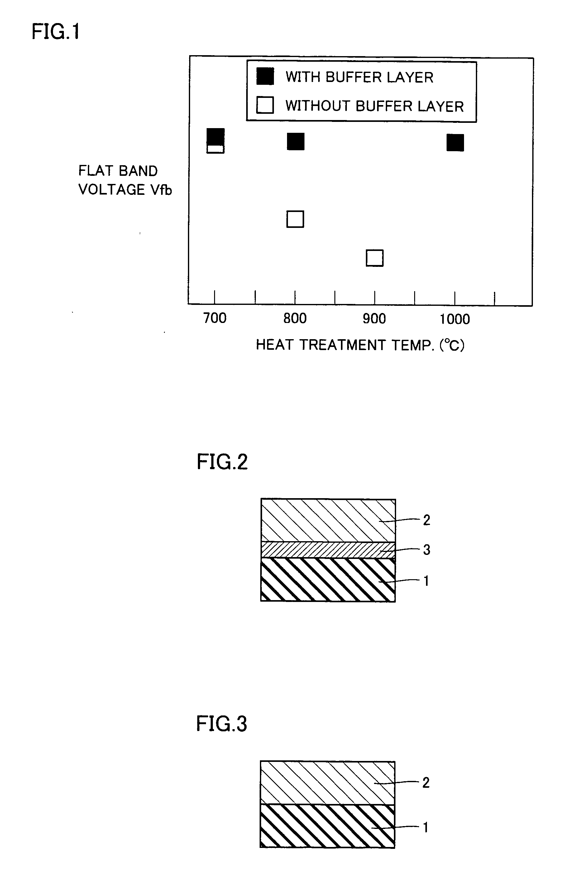
[0024] As a first embodiment according to the invention, the following experiment was performed for inspecting an effect of a buffer layer. Some samples of MISFETs were prepared. In these samples, an n-type silicon substrate was provided at its surface with a gate electrode made of TaSiN and a gate insulating film made of HfSiON. In some of the prepared samples, a buffer layer made of SiN and having a physical film thickness of 2 nm was interposed between the gate electrode and the gate insulating film. The other samples were not provided with a buffer layer. The samples with the buffer layer correspond to the semiconductor device according to the invention.

[0025] As exemplified herein, the semiconductor device according to the invention includes a semiconductor substrate, a gate insulating film formed in contact with an upper side of the semiconductor substrate, and a gate electrode made of metal nitride or metal nitride silicide and formed on the upper side of the gate insulating...

second embodiment

[0028] As a semiconductor device of a second embodiment according to the invention, a MISFET shown in FIG. 2 was prepared. This MISFET includes a gate insulating film 1 made of HfO2, a gate electrode 2 made of TiN and a buffer layer 3 which is made of a titanium film of 1 nm in thickness and is interposed between the gate insulating film and the gate electrode. Thus, in the semiconductor device of the second embodiment, gate electrode 2 contains Ti elements, gate insulating film 1 contains Hf elements and buffer layer 3 contains the titanium film.

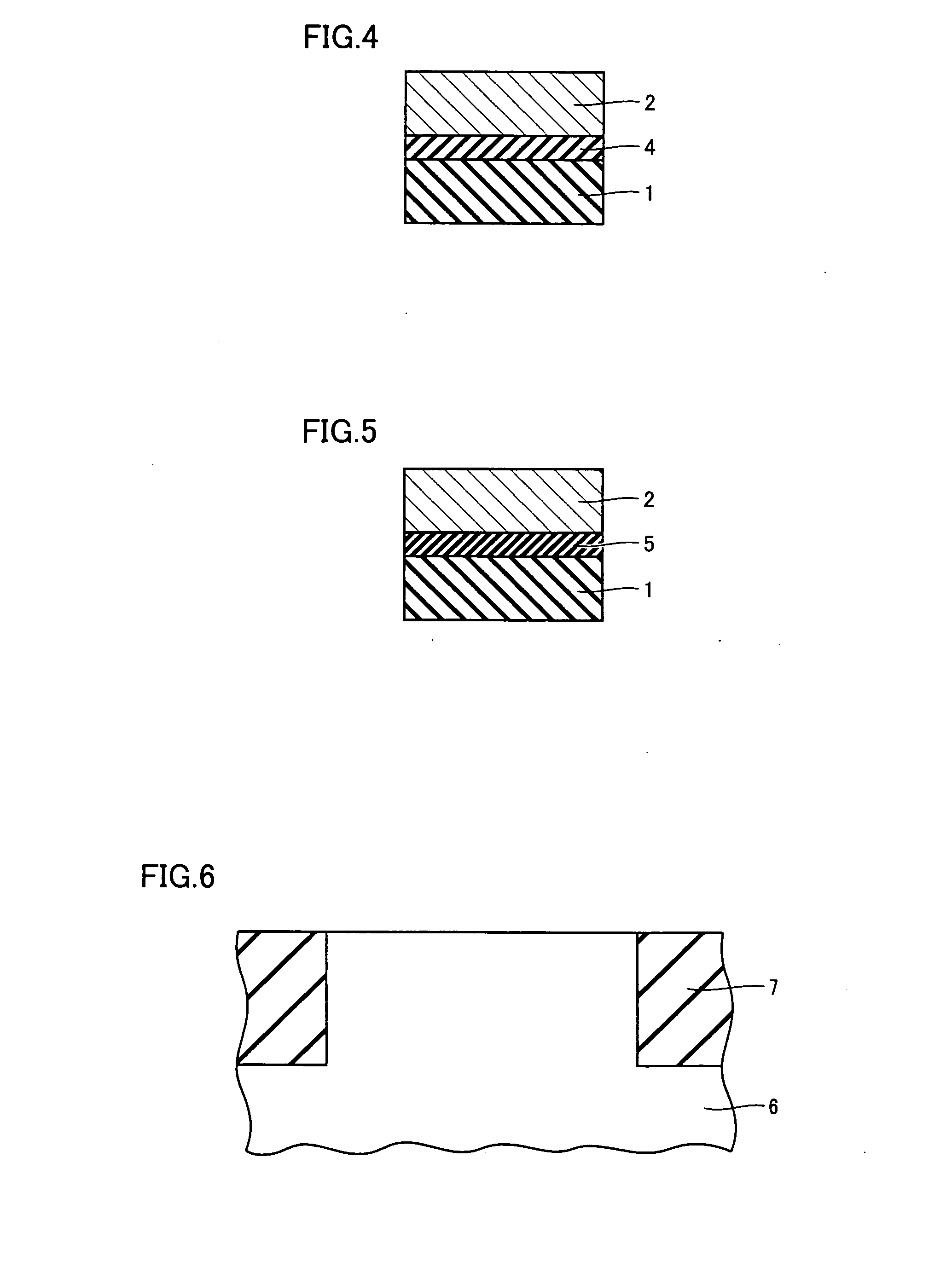
[0029] For comparison, a MISFET shown in FIG. 3 was prepared. This MISFET has the same structure as that shown in FIG. 2 except for that buffer layer 3 is not employed. Each of FIGS. 2 and 3 shows an interface between the gate insulating film and the gate electrode in the MISFET as well as a portion near it.

[0030] In the MISFET without a buffer layer, it was confirmed that a TiO2 film 4 was formed between gate insulating film 1 and gate e...

third embodiment

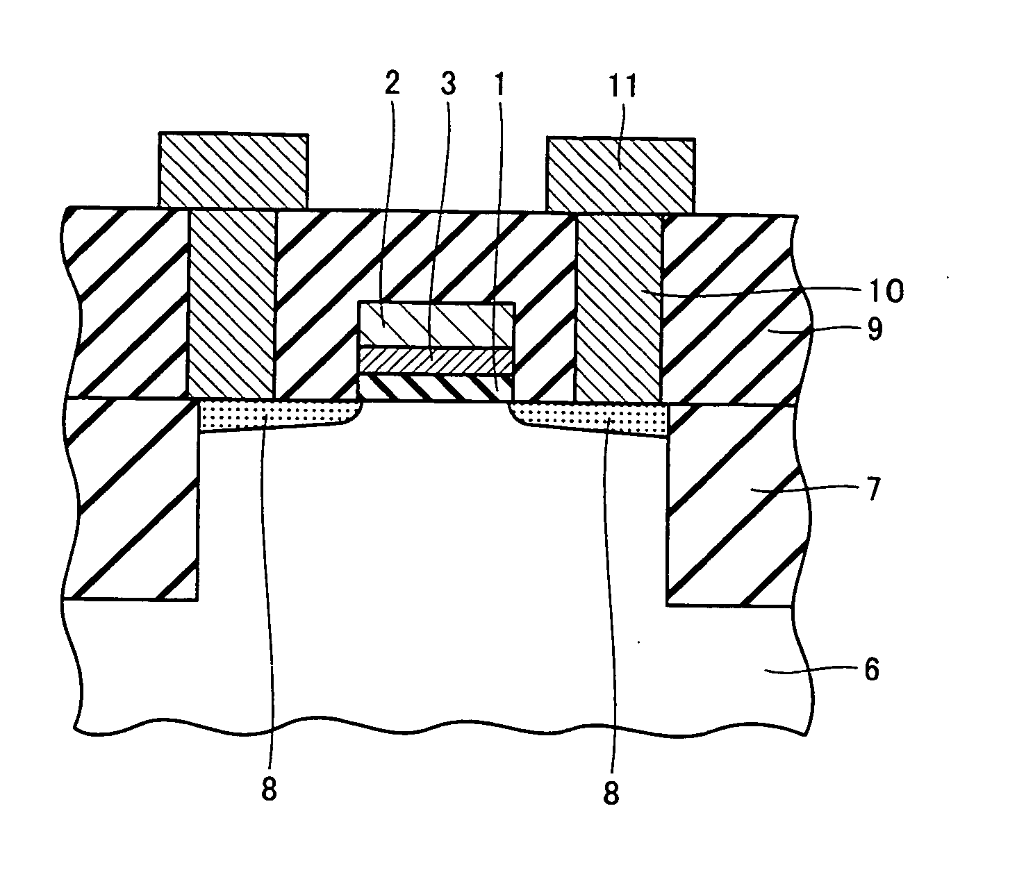
[0033] A MISFET was prepared as a semiconductor device of a third embodiment according to the invention. This MISFET includes a gate insulating film made of HfSiON and a gate electrode made of TiN. An SiN film is interposed as a buffer layer between the gate insulating film and the gate electrode.

[0034] An example of a method of manufacturing a semiconductor device according to the embodiment will now be described. First, as shown in FIG. 6, an element isolation region 7 of a STI (Shallow Trench Isolation) type is formed by a usual technique at a surface of a semiconductor substrate 6. As shown in FIG. 7, an HfSiON layer 51 for forming gate insulating film 1, an SiN film 53 for forming buffer layer 3 and TiN layer 52 for forming gate electrode 2 are successively deposited to form a layered structure. TiN layer 52 for forming the gate electrode contains nitrogen of which content is controlled in advance for adjusting the work function. The nitrogen content of TiN layer 52 is determi...


PUM


Abstract

The semiconductor device includes a semiconductor substrate, a gate insulating film formed in contact with an upper side of the semiconductor substrate, and a gate electrode formed on the upper side of the gate insulating film and made of metal nitride or metal nitride silicide. A buffer layer for preventing diffusion of nitrogen and silicon is interposed between the gate insulating film and the gate electrode. Preferably, the buffer layer has a thickness of 5 nm or less. In the case where gate electrode contains Ti elements, and the gate insulating film contains Hf elements, the buffer layer preferably contains a titanium film.

Description

BACKGROUND OF THE INVENTION [0001] 1. Field of the Invention [0002] The present invention relates to a semiconductor device and a method of manufacturing the same, and particularly to a semiconductor device which is required to operate with a low voltage as well as a method of manufacturing the same. [0003] 2. Description of the Background Art [0004] Transistors selectively attains on and off states, and a current that flows between a source and a drain in the on state, i.e., when a voltage is placed on the gate electrode will now be referred to as an “on current”. The magnitude of the on current is proportional to a quantity Q of electric charges induced in a channel region formed at a semiconductor substrate. This charge quantity Q is expressed as follows in connection with an effective film thickness EOT of a gate insulating film. Q∝Cinv×(Vg−Vt) where Vg represents a voltage between the gate electrode and the semiconductor substrate, Vt represents a threshold voltage and Cinv is...

Claims


Application Information

Patent Timeline
IPC IPC(8): H01L29/94
CPCH01L21/28176H01L29/495H01L29/4966H01L29/517H01L29/66575
Inventor YUGAMI, JIROINOUE, MASAOMORI, KENICHISAKASHITA, SHINSUKE
Owner RENESAS ELECTRONICS CORP
Why Eureka
Try Eureka