Optical element wafer and method for manufacturing optical element wafer, optical element, optical element module, electronic element wafer module, electronic element module, and electronic information device

Inactive Publication Date: 2010-04-01
SHARP KK
View PDF0 Cites 28 Cited by
  • Summary
  • Abstract
  • Description
  • Claims
  • Application Information

AI Technical Summary

Benefits of technology

[0049]Therefore, part or all of the side surface of the replica is buried in the respective recesses carved in the base to form the replica, so that the contacting area of the base and the replica becomes larger than the contacting area of the replica and the master mold and the contacting area of the base and the replica becomes larger than the contacting area of the replica and the stamper mold. Thus, release of the master mold and stamper mold can be performed smoothly and the thickness of the connecting portion between the planarized portions becomes thicker by an amount equal to the depth of the recess. As a result, it becomes possible to accurately form the replica and accurately form the upper and lower stamper molds. Furthermore, it becomes possible to solve the problem of the strength issue in forming a large-sized lens wafer. Furthermore, it becomes possible to solve the problem of residual the air bubbles by reducing the difference in level on the surface.
[0050]According to

Problems solved by technology

Therefore, a problem with regard to the strength may occur when a particularly large resin plate of the lens wafer 208 is manufactured.
If the air bub

Method used


Image

  • Optical element wafer and method for manufacturing optical element wafer, optical element, optical element module, electronic element wafer module, electronic element module, and electronic information device
  • Optical element wafer and method for manufacturing optical element wafer, optical element, optical element module, electronic element wafer module, electronic element module, and electronic information device
  • Optical element wafer and method for manufacturing optical element wafer, optical element, optical element module, electronic element wafer module, electronic element module, and electronic information device

Examples


embodiment 1

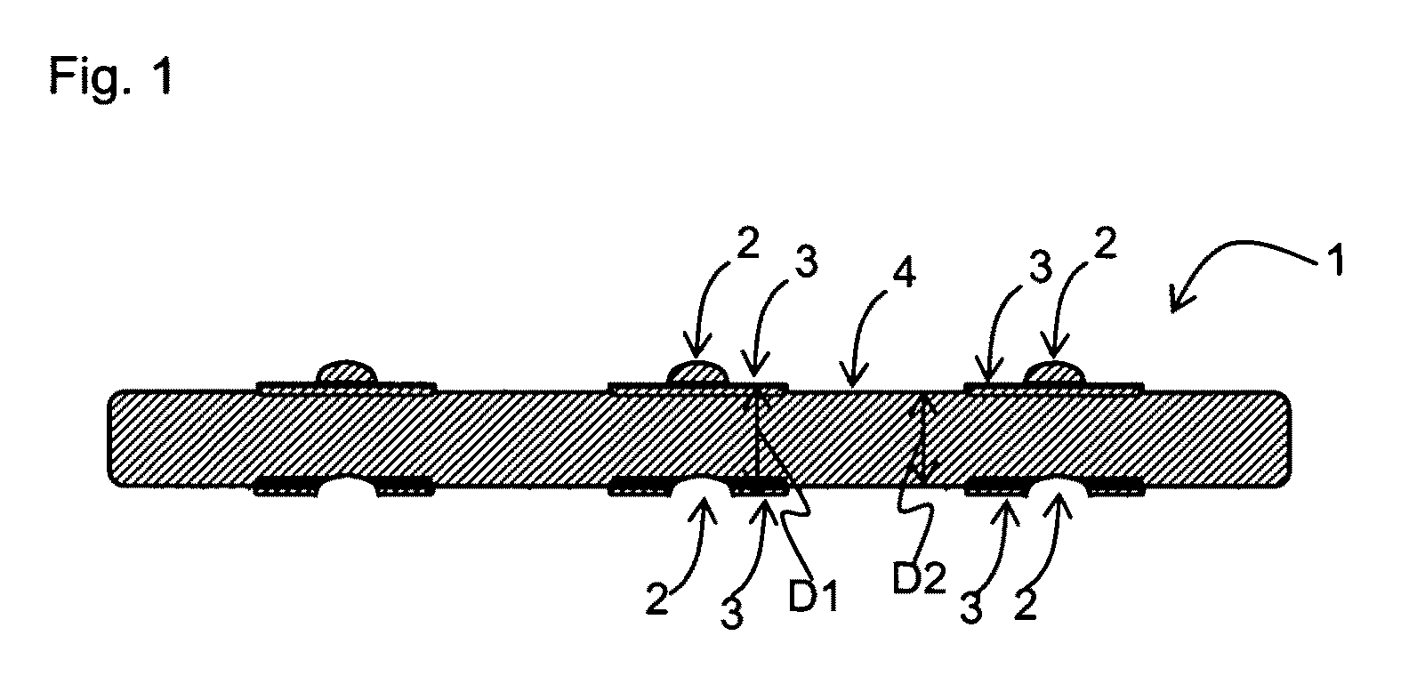
[0105]FIG. 1 is an essential part longitudinal cross sectional view illustrating an exemplary structure of a lens wafer according to Embodiment 1 of the present invention.

[0106]In FIG. 1, in a lens wafer 1 functioning as an optical element wafer of Embodiment 1, a plurality of lens areas 2 are formed as a plurality of optical element areas on either a front surface or a back surface thereof. A planarized portion 3 is disposed with a predetermined thickness on the outer circumference side of the lens area 2. A thickness D1 of the planarized portion 3 between adjacent lens areas 2 and a thickness D2 of a connecting portion 4 between the planarized portions 3 are within the ratio of 2:1 (2 / 1 or 1 / 2) to an equal ratio. Preferably, the thickness D1 of the planarized portion 3 between adjacent lens areas 2 is within the ratio of 4 / 3 (or 3 / 4) to an equal ratio with the thickness D2 of the connecting portion 4 between the planarized portions 3.

[0107]Herein, the resin thickness D2 between in...

embodiment 2

[0122]In Embodiment 2, a variation of a lens as an optical element, which is individualized from the lens wafer 1 as an optical element wafer formed by the upper and lower stamper molds 15 and 16 in Embodiment 1, will be described in detail. Furthermore, a variation of a lens module as an optical element module, in which the plurality of lenses are laminated, will be described in detail.

[0123]FIG. 6(a) is a longitudinal cross sectional view illustrating an exemplary variation of a lens individualized from the lens wafer of FIG. 1. FIG. 6(b) is a longitudinal cross sectional view illustrating an exemplary lens module in which a plurality of lenses are laminated. FIG. 6(c) is a top view of the second lens of FIG. 6(b). FIG. 6(d) is a top view of the first lens of FIG. 6(b). FIG. 6(e) is a longitudinal cross sectional view of a combination of the first lens and a light shielding holder. FIG. 6(f) is a longitudinal cross sectional view of a lens module of a combination of the exemplary ...

embodiment 3

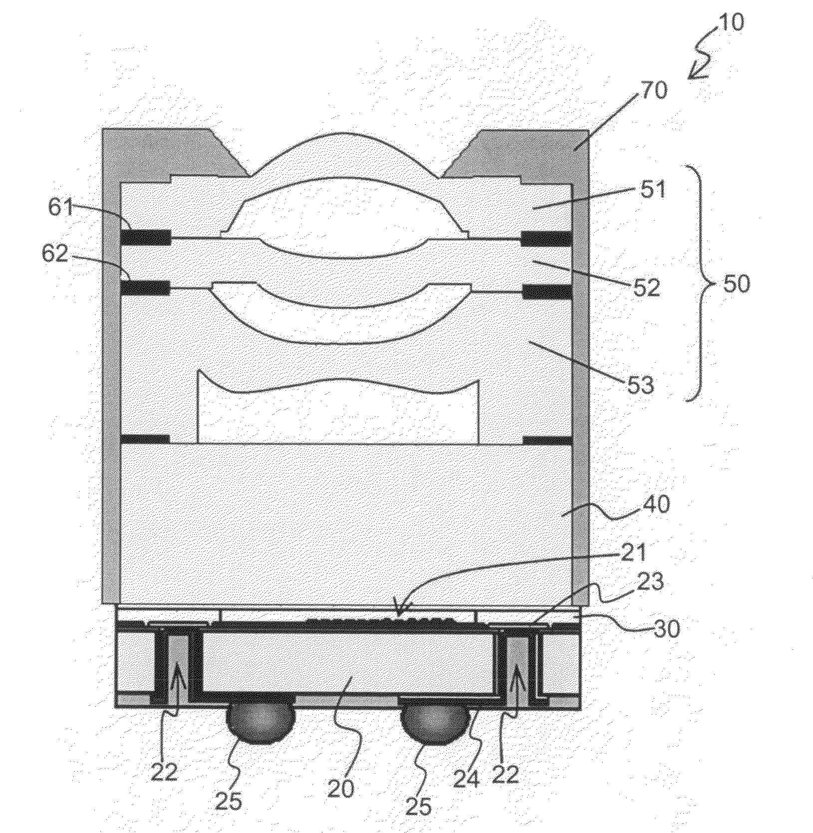
[0132]FIG. 7 is a longitudinal cross sectional view illustrating an exemplary essential part structure of a sensor module according to Embodiment 3 of the present invention.

[0133]In FIG. 7, a sensor module 10 as an electronic element module according to Embodiment 3 includes: an image capturing element 21, which includes a plurality of light receiving sections for performing photoelectric conversion on and capturing an image of image light from a subject, disposed at the center portion; an image capturing element chip 20 with a penetrating electrode 22 to the image capturing element 21; a resin adhesion layer 30 formed on the image capturing element chip 20 and between adjacent image capturing elements 21; a transparent support substrate 40, such as a glass plate, covering the image capturing element chip 20 and adhered and fixed on the resin adhesion layer 30; a lens module 50 provided to correspond to the image capturing element 21.

[0134]With regard to the image capturing element ...


PUM


Abstract

A method for manufacturing an optical element wafer according to the present invention, in which a plurality of optical elements are arranged in two dimensions, includes: a replica forming step of forming a replica, in which an optical element shape is formed on a front surface side, in each of a plurality of recesses formed in a base; a stamper mold forming step of forming a stamper mold using the optical element shape of the replica; and an optical element wafer forming step of transferring the optical element shape to an optical element material using the stamper mold to form an optical element wafer.

Description

[0001]This nonprovisional application claims priority under 35 U.S.C. §119(a) to Patent Applications No. 2008-249253 filed in Japan on Sep. 26, 2008, and No. 2009-199032 filed in Japan on Aug. 28, 2009, the entire contents of which are hereby incorporated by reference.BACKGROUND OF THE INVENTION[0002]1. Field of the Invention[0003]The present invention relates to: an optical element wafer, such as a lens wafer or an optical function element wafer, including a plurality of lenses as a plurality of optical elements for focusing incident light; a method for manufacturing the optical element wafer; an optical element individualized by simultaneous cutting from the optical element wafer; an optical element module individualized by simultaneous cutting from an optical element wafer module in which the plurality of optical element wafers are laminated; an electronic element wafer module, such as a sensor wafer module, which is a combination of an optical element or an optical element modul...

Claims


Application Information

Patent Timeline
IPC IPC(8): H04N5/335B29D11/00G02B3/08G02B7/00H01L31/12G02B3/00H01L27/14
CPCG02B7/02G02B13/0085H01L27/14618H04N5/2257H01L27/14683H01L27/14687H04N5/2253H01L27/14632H01L2224/13H01L2224/05548H01L2224/05573H01L2924/00014H01L2224/0554H04N23/54H04N23/57H01L2224/05599H01L2224/0555H01L2224/0556
Inventor KURIMOTO, HIDEYUKIYANO, YUJI
Owner SHARP KK
Why Eureka
Try Eureka