Embedded thin film sensors and methods of embedding thin film sensors

a technology of embedded thin film and sensors, which is applied in the direction of instruments, force/torque/work measurement apparatus, paper/cardboard containers, etc., can solve the problem that mounting the sensors to the outside of the mass of the material might not always be possibl

Active Publication Date: 2010-04-08
WISCONSIN ALUMNI RES FOUND
View PDF15 Cites 19 Cited by
  • Summary
  • Abstract
  • Description
  • Claims
  • Application Information

AI Technical Summary

Problems solved by technology

Moreover, due to the shape, size and / or use of the sensor and / or the device being sensed, mounting the sensors to the outside of the mass of the material might not always be possible.

Method used


Image

  • Embedded thin film sensors and methods of embedding thin film sensors
  • Embedded thin film sensors and methods of embedding thin film sensors
  • Embedded thin film sensors and methods of embedding thin film sensors

Examples


Embodiment Construction

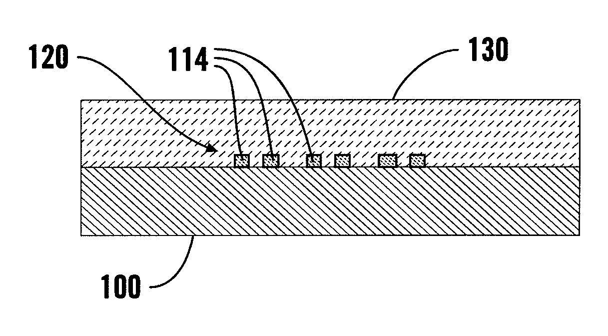
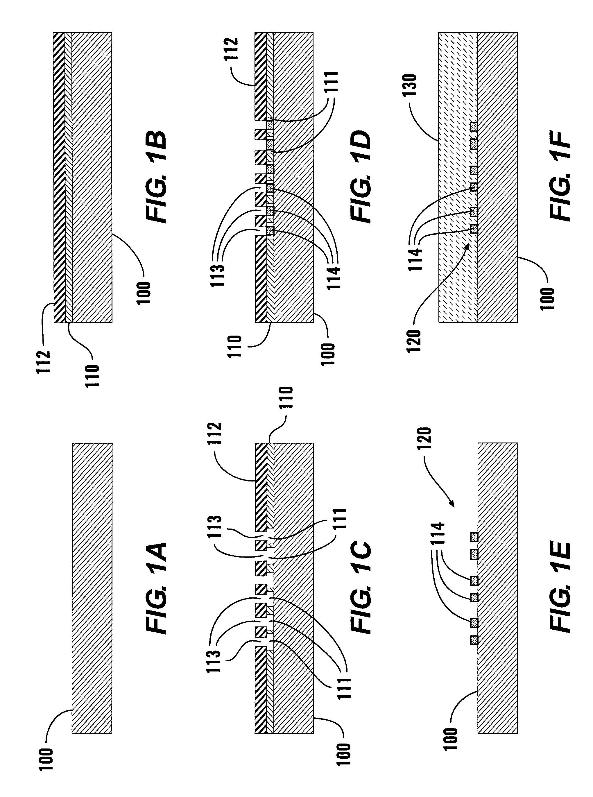
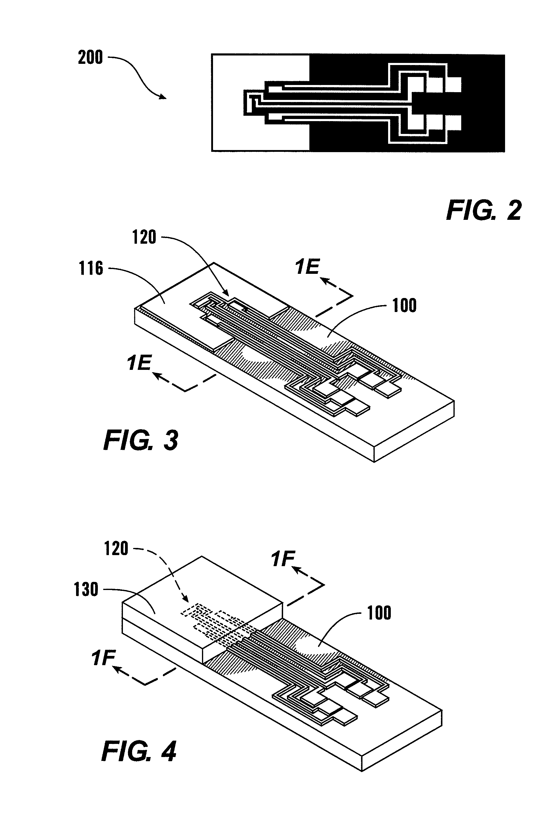
[0010]While the incorporated '700 and '995 published patent applications disclose methods for embedding sensors into high-melting-temperature matrix materials, those disclosed methods are either impractical or impossible without using electroplatable materials. For example, the sensors and methods disclosed in the incorporated '700 and '995 published patent applications may not be practical or usable with ceramics, i.e., it is difficult at best; if not impossible, to use these methods to embed a sensor in a ceramic mass. Often, sensors need to be embedded in non-electroplatable materials such as, for example, certain metals and ceramics such as, for example, sapphire or polycrystalline cubic boron nitride.

[0011]This invention provides a method for embedding a thin film sensor and / or device in a non-electroplatable material.

[0012]This invention separately provides a method for providing a ceramic structure around a thin film sensor and / or device.

[0013]This invention further provides ...


PUM

PropertyMeasurementUnit
temperatureaaaaaaaaaa
pressureaaaaaaaaaa
temperatureaaaaaaaaaa

Abstract

An embedded sensor or other desired device is provided within a completed structure through a solid-state bonding process (e.g., by diffusion bonding) and / or through a dynamic bonding process (e.g., by brazing). The embedded sensor or other desired device is provided on a substrate through any know or later-developed method (e.g., a photolithography or conductive ink printing process). A cover is then bonded to the substrate using a solid-state bonding process and / or a dynamic bonding process. The solid-state bonding process and / or dynamic bonding process may include providing heat and / or pressure to the substrate, the cover and / or a bonding agent (e.g., a filler metal or alloy) to bond the substrate and the cover together.

Description

[0001]The subject matter of this application was made with U.S. Government support awarded by the following agencies: NSF 0134583 and NSF 0330356. The United States has certain rights to this application.BACKGROUND[0002]1. Field of the Invention[0003]This invention relates to embedded thin film sensors and methods of embedding thin film sensors.[0004]2. Related Art[0005]Embedding sensors into a mass of material allows the sensors to sense the value of a parameter of the mass in a way that often is not possible with surface mounted sensors. Some material data, such as that relating to the internal thermal and mechanical properties of the material, can only be collected by in situ sensors. For example, internal temperature and strain data is obtained by embedding sensors into a component, with information from remote areas being extrapolated from an array of such sensors.[0006]Moreover, due to the shape, size and / or use of the sensor and / or the device being sensed, mounting the sensor...

Claims


Application Information

Patent Timeline
Patent Type & Authority Applications(United States)
IPC IPC(8): B26D7/27B32B37/00B23K1/00
CPCB26D1/0006B26D5/00Y10T156/10B26D7/27B26F1/44B26D7/00Y10T83/04Y10T83/849Y10T29/49103B23B51/00B23B2226/125B23B2226/69G01L5/0061
Inventor LI, XIAOCHUNDATTA, ARINDOMCHENG, XUDONG
Owner WISCONSIN ALUMNI RES FOUND
Why Eureka
Try Eureka