Silicon-base piezoelectric film sensor for biological micromass detection and its making process

A piezoelectric film and sensor technology, applied in special data processing applications, instruments, measuring devices, etc., can solve problems such as different resonance electrodes, insufficient sensitivity, and differences in resonance performance, and achieve the effect of increasing resonance frequency and detection sensitivity

Active Publication Date: 2007-10-03
SHANGHAI INST OF MICROSYSTEM & INFORMATION TECH CHINESE ACAD OF SCI
View PDF0 Cites 16 Cited by
  • Summary
  • Abstract
  • Description
  • Claims
  • Application Information

AI Technical Summary

Problems solved by technology

The disadvantage is that the sensitivity is not high enough, and the auxiliary equipment is expensive
At the same time, due to different resonant electrodes, different preparation methods and different material systems, the resonance performance of this type of device will vary greatly.

Method used


Image

  • Silicon-base piezoelectric film sensor for biological micromass detection and its making process
  • Silicon-base piezoelectric film sensor for biological micromass detection and its making process
  • Silicon-base piezoelectric film sensor for biological micromass detection and its making process

Examples


Embodiment 1

[0050] Embodiment 1: silicon-based piezoelectric thin film biosensor preparation, its steps are

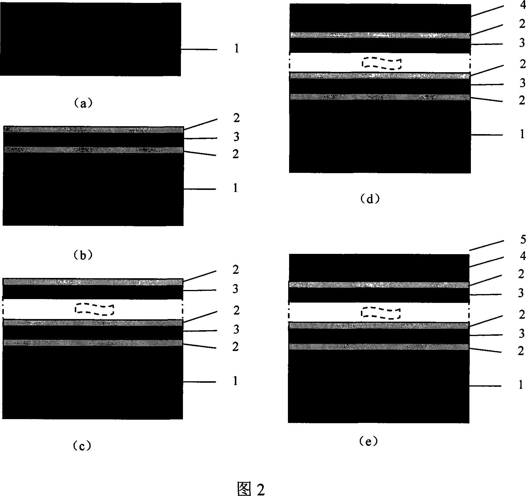
[0051] (1) The prepared piezoelectric resonator with multiple Bragg reflection layers. On a (100) oriented Si wafer with a diameter of 3 inches, a Pt / ZnO Bragg reflective layer was sputtered by multi-target magnetron sputtering. Before starting, evacuate to a background vacuum of 2×10 -4 Pa, and then heat the substrate Si wafer to 300°C. The sputtering power is DC 100W and RF 200W respectively; the sputtering gas flow is argon (Ar) 50sccm and argon (Ar):oxygen (O 2 ), 25:25sccm; the sputtering working pressure is 1.7×10 -1 Pa and 1.8×10 -1 Pa; The Bragg reflective layer was prepared by multi-target continuous sputtering. Each film is hundreds of nanometers thick. [Figure 2(a)~(c)].

[0052] (2) Preparation of the piezoelectric thin film layer: the piezoelectric thin film is prepared on the Bragg reflection layer. Using a multi-target magnetron sputtering apparatus, the pre...

Embodiment 2

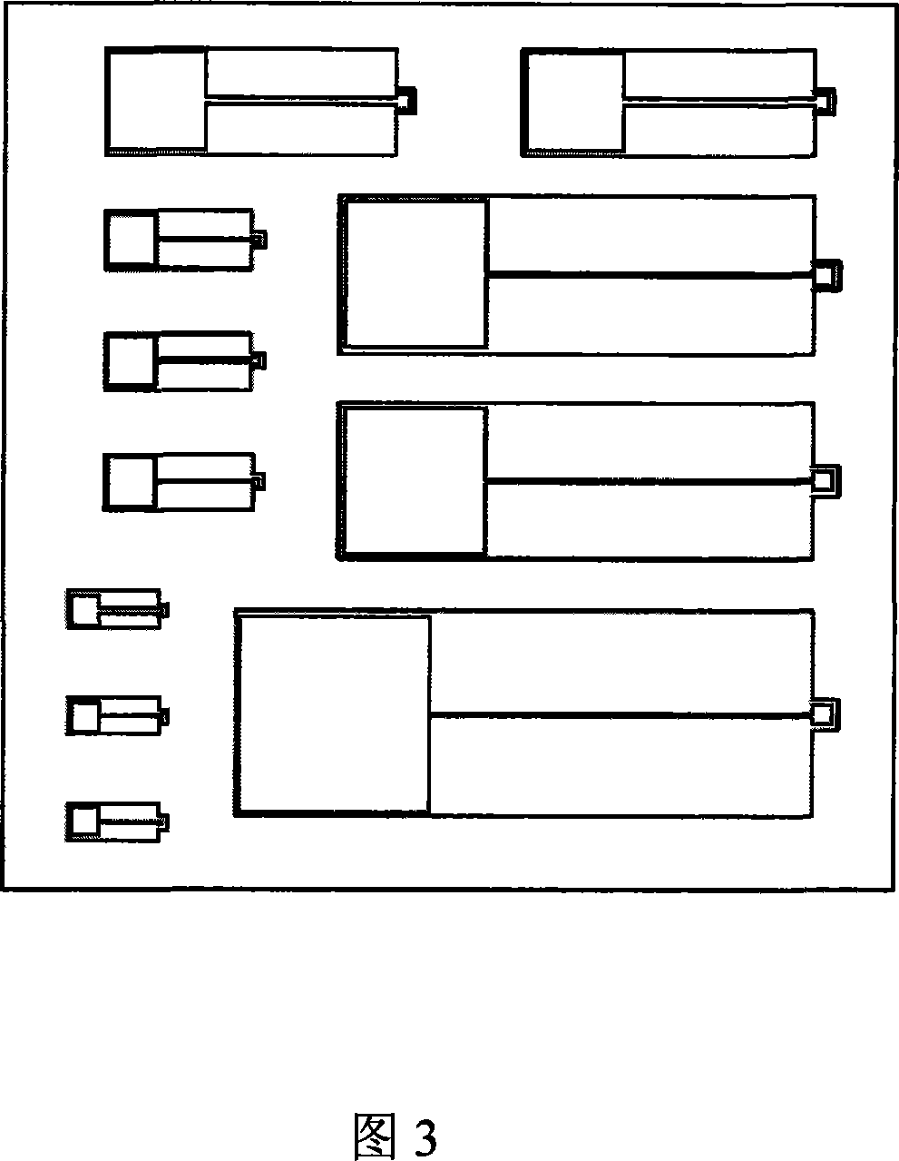
[0060] On the basis of the entire thin film resonator device preparation process described in Example 1, the preparation method of the Bragg layer in the process step (1) is changed: the sputtering gas flow rate of sputtering Pt and ZnO is respectively adjusted to 100 sccm of argon and 50 sccm of oxygen , argon 50sccm, and then improve the sputtering working pressure to be 0.40Pa and 0.37Pa respectively; In the process step (2), the piezoelectric thin film layer is also correspondingly changed to the oxygen and argon flow rate as oxygen 50sccm, argon 50sccm, to improve the sputtering work The air pressure is 0.37Pa. And change the thickness of the film to change the characteristic resonant frequency; in the process step (5), a better graphic electrode structure (Figure 7) is used to prepare a silicon-based piezoelectric thin film biosensor, and more accurately realize the biomolecules after binding. The shift of the resonance peak. (Figure 8)


PUM

PropertyMeasurementUnit
thicknessaaaaaaaaaa
thicknessaaaaaaaaaa
thicknessaaaaaaaaaa

Abstract

The present invention is silicon-base piezoelectric film sensor for biological micro mass detection and its making process. The silicon-base piezoelectric film sensor is made through the following steps: depositing Bragg reflection layer of one quarter wavelength thickness on a (100) orientation silicon chip, depositing one piezoelectric film layer and one gold electrode layer, forming electrode structure matching standard microwave measurement, and annealing. During detection, serial biological probes are coated on the silicon-base piezoelectric film sensor and the sampled biological micro mass is combined so as to measure the changing sensor resonance frequency and to obtain the biological micro mass. The present invention has combination between multifunctional integral sensing technology and modern biotechnology to complete biological micro mass measurement in high flux, high specificity and high sensitivity.

Description

technical field [0001] The present invention relates to a silicon-based piezoelectric thin film sensor applied to the detection of biological micro-mass and a manufacturing method thereof, more precisely relates to a silicon-based piezoelectric thin-film sensor applied to the detection of biological micro-mass, which embodies multifunctional integrated sensing The application of technology combined with modern biotechnology. It belongs to the field of biosensor production. Background technique [0002] For nearly half a century, the research and development of biosensors has been paid attention to by people, and a variety of sensors (such as electrochemical sensors, thermal biosensors, piezoelectric biosensors, semiconductor biosensors and optical biosensors, etc.) have emerged as the times require. [0003] The principle of specific binding between biological macromolecules (such as hybridization of nucleic acid molecules, receptor-ligand binding and antigen-antibody react...

Claims


Application Information

Patent Timeline
Patent Type & Authority Applications(China)
IPC IPC(8): G01N27/00G01N29/14G06F19/00
Inventor 宋志棠刘卫丽言智张挺程建功封松林赖立辉陈建照
Owner SHANGHAI INST OF MICROSYSTEM & INFORMATION TECH CHINESE ACAD OF SCI
Why Eureka
Try Eureka