Dielectric mesh isolated phase change structure for phase change memory

a phase change memory and dielectric mesh technology, applied in the field of memory devices, can solve the problems of electrical and mechanical reliability of the cell, endurance of the dimension phase change device, stress at the interface and within the gst material, etc., and achieve the effect of improving the memory cell and reducing the grain siz

a phase change memory and dielectric mesh technology, applied in the field of memory devices, can solve the problems of electrical and mechanical reliability of the cell, endurance of the dimension phase change device, stress at the interface and within the gst material, etc., and achieve the effect of improving the memory cell and reducing the grain siz

US20100084624A1Active Publication Date: 2010-04-08GLOBALFOUNDRIES US INC

Image

  • Dielectric mesh isolated phase change structure for phase change memory
  • Dielectric mesh isolated phase change structure for phase change memory
  • Dielectric mesh isolated phase change structure for phase change memory

Examples


Embodiment Construction

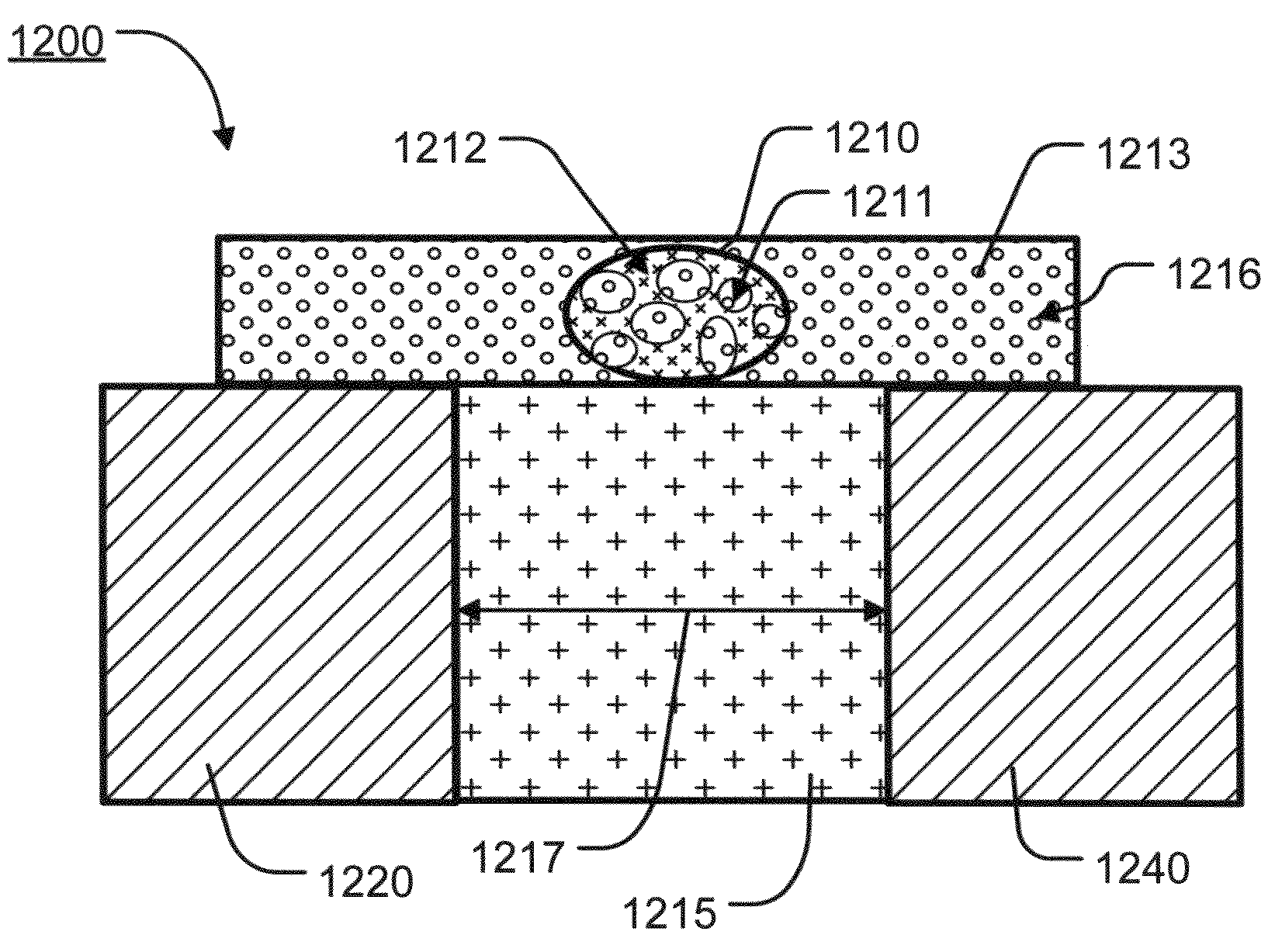
[0038]The following description of the disclosure will typically be with reference to specific structural embodiments and methods. It is to be understood that there is no intention to limit the disclosure to the specifically disclosed embodiments and methods, but that the disclosure may be practiced using other features, elements, methods and embodiments. Preferred embodiments are described to illustrate the present disclosure, not to limit its scope, which is defined by the claims. Those of ordinary skill in the art will recognize a variety of equivalent variations on the description that follows. Like elements in various embodiments are commonly referred to with like reference numerals.

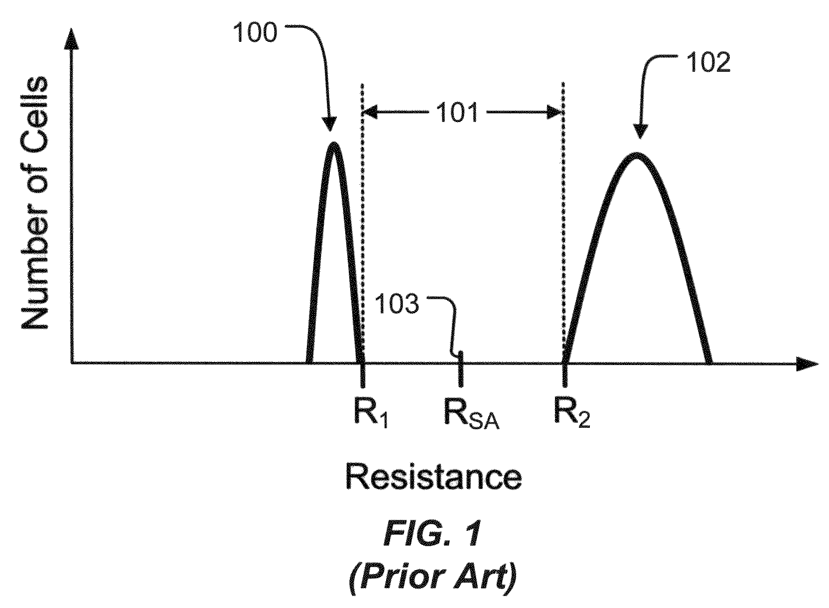
[0039]In phase change memory, data is stored by causing transitions in an active region of the phase change material between amorphous and crystalline phases. FIG. 1 is a graph of memory cells having one of two states (storing a single bit of data), a low resistance set (programmed) state 100 and a ...


PUM

PropertyMeasurementUnit
phase changeaaaaaaaaaa
concentrationaaaaaaaaaa
electrical resistivityaaaaaaaaaa

Abstract

A method for manufacturing a memory device, and a resulting device, is described using silicon oxide doped chalcogenide material. A first electrode having a contact surface; a body of phase change memory material in a polycrystalline state including a portion in contact with the contact surface of the first electrode, and a second electrode in contact with the body of phase change material are formed. The process includes melting and cooling the phase change memory material one or more times within an active region in the body of phase change material without disturbing the polycrystalline state outside the active region. A mesh of silicon oxide in the active region with at least one domain of chalcogenide material results. Also, the grain size of the phase change material in the polycrystalline state outside the active region is small, resulting in a more uniform structure.

Description

PARTIES TO A JOINT RESEARCH AGREEMENT[0001]International Business Machines Corporation, a New York corporation, and Macronix International Corporation, Ltd., a Taiwan corporation, are parties to a Joint Research Agreement.BACKGROUND OF THE INVENTION[0002]1. Field of the Invention[0003]The present invention relates to memory devices based on chalcogenide materials, and methods for manufacturing such devices.[0004]2. Description of Related Art[0005]Phase change based memory materials, like chalcogenide based materials and similar materials, can be caused to change phase between an amorphous state and a crystalline state by application of electrical current at levels suitable for implementation in integrated circuits. The generally amorphous state is characterized by higher electrical resistivity than the generally crystalline state, which can be readily sensed to indicate data. These properties have generated interest in using programmable resistive material to form nonvolatile memory...

Claims


Application Information

Patent Timeline
08 Apr 2010
Publication
US20100084624A1
IPC
H01L47/00; H01L21/06
CPC
H01L45/06; H01L45/1226; H01L45/1233; H01L45/1641; H01L45/144; H01L45/1625; H01L45/1246
Inventors
LUNG, HSIANG-LAN; CHEN, CHIEH FANG