Semiconductor light emitting apparatus

a technology of light-emitting apparatus and semiconductors, which is applied in the direction of semiconductor devices, electrical devices, basic electric elements, etc., can solve the problems of color unevenness, difficulty in maintaining, and emission of white light by color mixture of light emitted, and achieve the effect of preventing color unevenness

Inactive Publication Date: 2010-04-08
STANLEY ELECTRIC CO LTD
View PDF13 Cites 23 Cited by
  • Summary
  • Abstract
  • Description
  • Claims
  • Application Information

AI Technical Summary

Benefits of technology

[0009]Another method for forming a phosphor-containing layer can include coating a top surface of a semiconductor light emitting element with a transparent resin such as an epoxy resin, a silicone resin and the like in which phosphor particles have been dispersed (that is collectively referred to as a “wavelength converting member” hereinafter), by means of a dispenser. In this case, the wavelength conversion member is coated over the top surface of the semiconductor light emitting element so as not to run over the top surface of the element. This configuration can remarkably suppress color unevenness when compared with the configuration of FIG. 1.
[0011]The presently disclosed subject matter was devised in view of these and other features, characteristics, and problems and in association with the conventional art. According to an aspect of the presently disclosed subject matter, a semiconductor light emitting apparatus for emitting a desired colored light by coating the top surface thereof with a wavelength conversion member can be configured to prevent color unevenness from occurring due to the unevenness of the coating thickness of the wavelength conversion member.

Problems solved by technology

In addition, it is difficult to maintain over a long period of time the emission of white light by color mixture of light emitted from three colored LEDs.
This method, however, poses problems including color unevenness where the color of emitted light is different at the center just above the light emitting surface of the semiconductor light emitting element from the color at the outer peripheral portion thereof.
This color unevenness may make it difficult for application of the light in headlights for vehicles or for general-purpose lighting fixtures.
The method for coating the top surface of a semiconductor light emitting element with the wavelength conversion member by means of a dispenser, however, has a problem in which the wavelength conversion member cannot sufficiently be spread over the top surface of the semiconductor light emitting element up to the respective corner areas, for example.
Accordingly, the method for forming a phosphor-containing layer by coating the top surface of a semiconductor light emitting element with a wavelength conversion member has a problem in that color unevenness may occur due to the unevenness of the coating thickness.

Method used


Image

  • Semiconductor light emitting apparatus
  • Semiconductor light emitting apparatus
  • Semiconductor light emitting apparatus

Examples


second exemplary embodiment

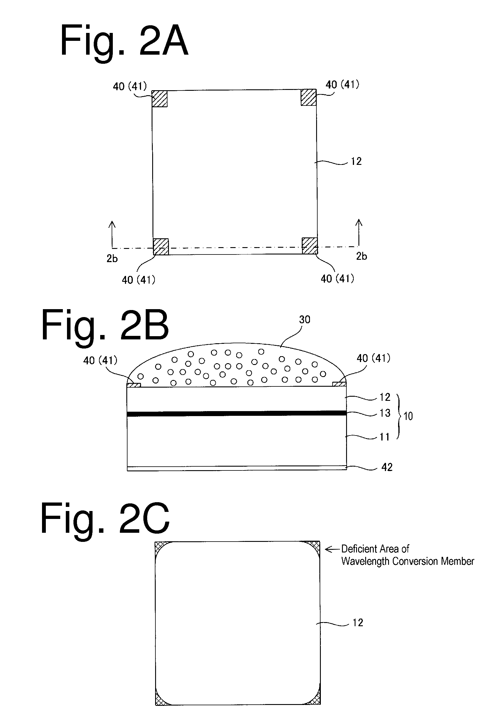
[0062]FIG. 6A is a top plan view illustrating the top plan view of the semiconductor light emitting apparatus of a second exemplary embodiment made in accordance with principles of the presently disclosed subject matter, and FIG. 6B is a cross-sectional view taken along line 6b-6b in FIG. 6A. Note that the phosphor-containing layer is omitted in FIG. 6A for facilitating understanding of the subject matter.

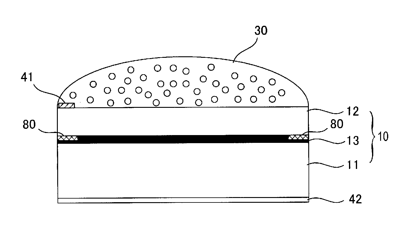
[0063]The basic configuration of the semiconductor light emitting apparatus of the present exemplary embodiment can be the same as that of the first exemplary embodiment. Specifically, the semiconductor layer 12 including the light emitting layer can be bonded onto the opaque support substrate 11 made of Si or Ge via a metal layer 13. The metal layer 13 can function as a light reflecting layer in addition to the bonding layer for the support substrate 11 and the semiconductor layer 12. The dome-shaped phosphor-containing layer 30 can be formed by dropping a wavelength conversion me...

third exemplary embodiment

[0076]FIG. 8 shows a cross sectional view of a third exemplary embodiment of a semiconductor light emitting apparatus of the presently disclosed subject matter. The basic configuration of the semiconductor light emitting apparatus of the present exemplary embodiment can be the same as that of the first exemplary embodiment. Specifically, the semiconductor layer 12 including the light emitting layer can be bonded onto the opaque support substrate 11 made of Si or Ge via a metal layer 13. The metal layer 13 can function as a light reflecting layer in addition to the bonding layer for the support substrate 11 and the semiconductor layer 12. The dome-shaped phosphor-containing layer 30 can be formed by dropping a wavelength conversion member that is prepared by dispersing a phosphor in a transparent resin, on the top of the semiconductor element 10. An electrode pad 41 can be provided on the top surface of the semiconductor layer 12 and a rear electrode 42 can be provided on the rear su...


PUM


Abstract

A semiconductor light emitting apparatus for emitting a desired colored light by coating the top surface thereof with a wavelength conversion member prevents the color unevenness from occurring due to the unevenness of the coating thickness of the wavelength conversion member. The semiconductor light emitting apparatus can include a semiconductor layer having a light emitting layer with a light emitting surface having at least one corner area, a supporting substrate configured to support the semiconductor layer, and a wavelength conversion material layer formed on top of the semiconductor layer, the wavelength conversion layer having a thickness thinner from a center portion of the semiconductor layer to an outer peripheral portion. The at least one corner area can include a non-emitting portion where light cannot be projected. The non-emitting portion can be a light shielding portion, a non-light emission portion or a current confined portion.

Description

[0001]This application claims the priority benefit under 35 U.S.C. §119 of Japanese Patent Application No. 2008-258284 filed on Oct. 3, 2008, which is hereby incorporated in its entirety by reference.TECHNICAL FIELD[0002]The presently disclosed subject matter relates to a semiconductor light emitting apparatus, and in particular, to a semiconductor light emitting apparatus that can utilize a wavelength converting material such as a phosphor to emit white light wherein unevenness in emission color can be reduced or prevented.BACKGROUND ART[0003]Light emitting diodes (hereinafter, referred to as “LED”) can be used with or incorporated in various devices including a tail light for vehicles, indication lamps or backlighting devices for various display devices and mobile equipment such as cellular phones. The growth in demand for such LED devices is expected to increase in the field of headlights for vehicles, backlights for liquid crystal display devices, general lighting fixtures and t...

Claims


Application Information

Patent Timeline
Patent Type & Authority Applications(United States)
IPC IPC(8): H01L33/00H01L33/02H01L33/06H01L33/14H01L33/32H01L33/44H01L33/48H01L33/50H01L33/56H01L33/62
CPCH01L33/145H01L33/20H01L33/38H01L33/508H01L2933/0016H01L2924/3025H01L2224/8592H01L2224/48091H01L2924/00014H01L2924/00
Inventor UENO, KAZUHIKOEBISUTANI, TAKASHI
Owner STANLEY ELECTRIC CO LTD
Why Eureka
Try Eureka