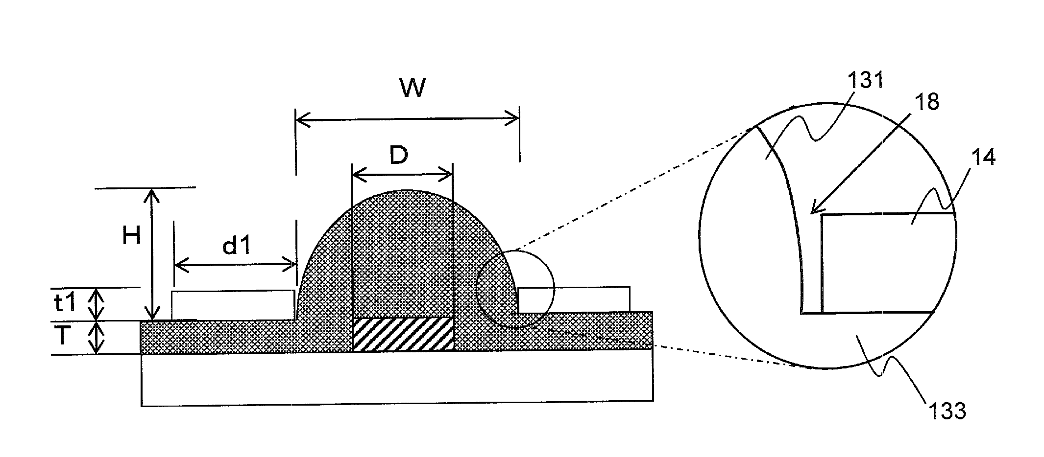
[0054]The thickness T of the thin film portion 133 can be equal to or less than the thickness of the LED element 13, and in one exemplary embodiment it can be 0.1 mm or smaller. If the thickness of the thin film portion 133 exceeds the thickness of the LED element, the advantageous effects of the formation of the hemispherical convex portion 131 or the
equalization of the
optical path length may be hampered.
[0055]The reflective portion 14 can reflect light emitted from the resin layer 13 as well as can shield the light exiting outside at the interface between itself and the resin layer 13. The reflective portion 14 may be formed from a reflective material having such a function, a material totally reflecting light (such as a
metal member or a mirror-finished member), or a
diffusion reflection material. In particular, a
diffusion reflection material, specifically a white reflection material is possible. If the reflective portion 14 is formed from a diffusion reflection material, the light generated from the thin film portion 133 of the resin layer 13 can be diffused to be directed to the convex portion 131, so that the mixing with the light directed upward from the LED element 12 can be effectively achieved as well as the production of the reflective portion 14 is facilitated.
[0056]Specifically, examples of the diffusion reflection material may include white resins prepared by mixing a white filler such as TiO2, Al2O3, AlN, SiO2, ZnO, etc. with a resin such as a
silicone resin, a
hybrid resin of
epoxy and
silicone, an
epoxy resin, a urethane resin, etc. If the reflective portion 14 is formed by
coating, it is possible to select a resin with an improved thixotropic property that facilitates the
coating and has a favorable shape retention property after the layer formation. If the reflective portion 14 is formed by adhesion, examples of the reflective portion 14 may include white reflective plates formed from a
ceramic material (Al2O3 or the like), a plastic material containing white filler (TiO2 or the like), etc.
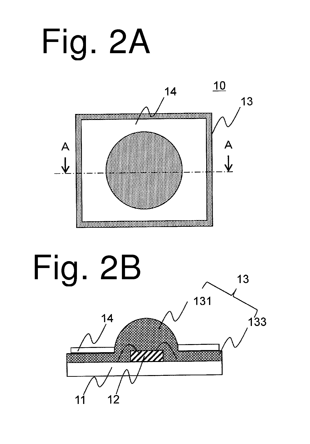
[0057]The reflective portion 14 can be formed over the thin film portion 133 of the resin layer 13 and outside the area of the convex portion 131. The thickness t1 of the reflective portion 14 in an exemplary embodiment can be 0.2 mm or more, and in another exemplary embodiment it can be 0.5 mm or more. If the thickness t1 of the reflective portion 14 is set to 0.2 mm or more, the light from the thin film portion 133 of the resin layer 13 disposed below the reflective portion 14 can be almost completely shielded by the reflective portion 14. The reflective portion 14 can ideally be provided over the entire surface of the thin film portion 133, but is not limitative. The width d1 from the outer
peripheral of the convex portion 131 can be 0.2 mm or more in one exemplary embodiment, and can be 0.5 mm or more in another exemplary embodiment. If the width d1 of the reflective portion 14 is set to 0.2 mm or more, the light from the thin film portion 133 of the resin layer 13 can be sufficiently shielded by the reflective portion 14. In addition to this, the light from the thin film portion 133 of the resin layer 13 can be reflected by the same to the convex portion of the resin layer 13, so as to mix it with the light from the LED element 12.
[0058]The reflective portion 14 is not required to be in contact with the outer periphery of the convex portion 131. As shown in the enlarged view in FIG. 3, there may be a gap 18 between the side surface of the reflective portion 14 and the outer periphery of the convex portion 131. Part of the light emitted from the thin film portion 133 of the resin layer 13 exposed to the gap 18 can be reflected by side surface of the reflective portion 14 and enter the convex portion 131 of the resin layer 13. Another part of the light can be directly mixed with the light emitted from the convex portion 131 of the resin layer 13. This can suppress the color unevenness. The allowable distance of the gap 18 may vary depending on the thickness of the convex portion 131 of the resin layer 13 and / or the thickness of the reflective portion 14, and in one exemplary embodiment it can be 0.25 mm or less.
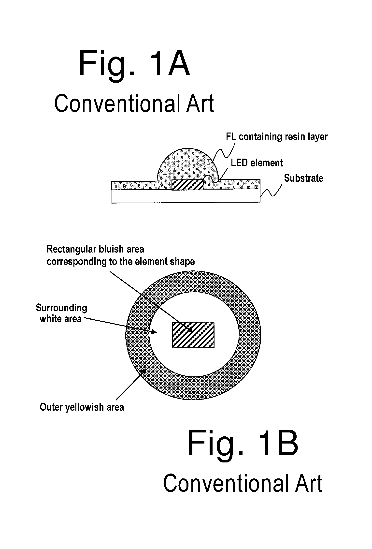
[0059]Next, the principle of suppressed or prevented color unevenness will be described with reference to FIG. 4A. In FIG. 4A, the trajectory of light generated from the thin film portion 133 of the resin layer 13 (surrounding yellowish light) is illustrated by a dot line, and the trajectory of light directed just above the LED device 12 (rectangular bluish light area) is illustrated by a dashed line. As illustrated, the light-emitting device of the present exemplary embodiment can be configured such that the light emitted from the top surface of the LED element 12 can be diffused radially and projected with almost the same color (for example, white) due to the equal
optical path length within the convex portion 131 of the resin layer 13. However, the luminance of light emitted at the center of the top surface of the LED element 12 is the maximum, and the
light emission color just above the LED element may be predominantly bluish. Further, the light emitted sideward from the LED element can cause the thin film portion 133 of the resin layer 13 to emit light, and the light emission color at that area may be predominantly yellowish. In the presently disclosed
subject matter, the light from the thin film portion 133 of the resin layer 13 cannot be projected directly outside (upward direction in the drawing) due to the reflective portion 14 formed thereabove. Accordingly, the light can be reflected at the interface between the thin film portion 133 of the resin layer 13 to be directed to the convex portion 133 disposed at the center of the device. Therefore, the yellowish light thus directed and the bluish light upward from the LED element 12 can be mixed together, so as to provide the resulting
white light from the convex portion 133. Accordingly, the rectangular bluish light directly above the LED element 12 and the yellowish light at the surrounding area can be prevented from occurring, thereby obtaining light emission without color unevenness.

