Boost Device for Voltage Boosting

Active Publication Date: 2010-04-08
HUNGKUANG UNIV
View PDF6 Cites 10 Cited by
  • Summary
  • Abstract
  • Description
  • Claims
  • Application Information

AI Technical Summary

Benefits of technology

[0016]Therefore, an object of the present invention is to provide a boost device that has relatively high bo

Problems solved by technology

1. When the switch 12 is in the OFF-state, a voltage across the switch 12 is substantially equal to the output voltage. Therefore, if the switch 12 is implemented as a MOSFET device, a relatively large conducting impedance is exhibited by the MOSFET device, thereby resulting in a relatively large conduction loss.
2. When the switch 12 is switched from the OFF-state to the ON-state, a reverse bias surge current is generated to flow through the switch 12 that causes serious switching loss, thereby reducing power transformation efficiency.
3. The conventional boost device has a relatively small boost ratio due to the presence of the inductor 11. Therefore, an input voltage converted from solar energy or supplied by a rechargeable battery set of a motor-driven vehicle is not suitably boosted by the conventional boost

Method used


Image

  • Boost Device for Voltage Boosting
  • Boost Device for Voltage Boosting
  • Boost Device for Voltage Boosting

Examples


Embodiment Construction

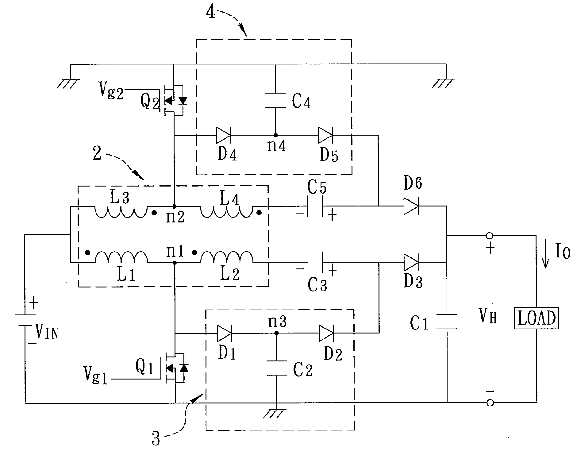
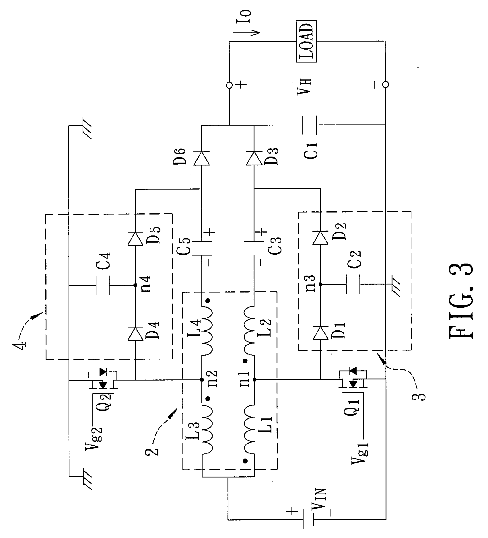
[0056]Referring to FIG. 3, an embodiment of a boost device is shown to be adapted for boosting an input voltage (VIN) supplied by an external source to an output voltage (VH). The boost device includes a transformer 2, a first switch (Q1), a second switch (Q2), an output capacitor (C1), a first switching circuit 3, a second switching circuit 4, a first boost capacitor (C3), a second boost capacitor (C5), a first output diode (D3), and a second output diode (D6).

[0057]The transformer 2 includes first, second, third and fourth windings (L1, L2, L3, L4) wound around an iron core (not shown). A winding ratio of the first, second, third and fourth windings (L1, L2, L3, L4) is equal to 1:N:1:N. Each of the first, second, third and fourth windings (L1, L2, L3, L4) has a polarity end and a non-polarity end. The polarity end of the first winding (L1) is adapted to be coupled to the external power source, and is coupled to the non-polarity end of the third winding (L3). The non-polarity end o...


PUM


Abstract

A boost device boosts an input voltage to an output voltage across an output capacitor, and includes first and second output diodes coupled to the output capacitor, and a transformer coupled to first and second switches, first and second switching circuits, and to the first and second output diodes, and receiving the input voltage. The first and second switches are operated alternately in an ON-state, and have overlapping duty cycles. The first and second switching circuits are operable to suppress conduction losses for the first and second switches. The transformer has a bi-directional magnetic circuit. Electric energy is transformed through induced currents of the transformer, and a small amount of energy attributed to an exciting current of the transformer is used for voltage boosting, thereby attaining a relatively high output power.

Description

BACKGROUND OF THE INVENTION[0001]1. Field of the Invention[0002]The invention relates to a boost device, more particularly to a DC-to-DC boost device.[0003]2. Description of the Related Art[0004]Referring to FIG. 1, a conventional boost device is shown to include an inductor 11, a switch 12, a diode 13, and a capacitor 14. The inductor 11 has a first end coupled to an external power source, and a second end. The switch 12, such as a semiconductor power switch, has a first terminal coupled to a common node between the second end of the inductor 11 and an anode of the diode 13, a second terminal coupled to ground, and a control terminal for receiving an external control signal such that the switch 12 is operable between an ON-state and an OFF-state in response to the external control signal. The capacitor 14 is coupled between a cathode of the diode 13 and ground.[0005]When the switch 12 is operated in the ON-state, a current from the external power source flows through the inductor 1...

Claims


Application Information

Patent Timeline
IPC IPC(8): H02M3/156
CPCH02M2003/1586H02M3/1584H02M3/1586
Inventor DUAN, ROU-YONGLUO, RONG-DA
Owner HUNGKUANG UNIV
Why Eureka
Try Eureka