Semiconductor device having delay control circuit

a control circuit and semiconductor technology, applied in the field of semiconductor devices, can solve the problems of increasing the frequency of a clock signal, not always constant delay amount of each delay element, and malfunction of the device, so as to prevent performance degradation, increase the circuit size and power consumption, and reduce the effect of delay delay

Inactive Publication Date: 2010-04-08
LONGITUDE LICENSING LTD
View PDF4 Cites 24 Cited by
  • Summary
  • Abstract
  • Description
  • Claims
  • Application Information

AI Technical Summary

Benefits of technology

[0013]As described above, according the present invention, the variation of the delay amount due to PVT variation can be properly corrected because the delay amount of the delay control circuit is set based on a difference in propagation speed between two delay circuits having different operation conditions. Consequently, it is possible to prevent perfor

Problems solved by technology

However, in a semiconductor memory device such as a DRAM (Dynamic Random Access Memory), increasing a frequency of a clock signal cannot always lead to a high speed operation of its memory cell array because the memory cell array performs an analog operation.
However, a delay amount of each of the delay elements is not always constant, and varies according to various conditions.
The larger the PVT variation is, the more the operation timing is deviated from its design value, which causes a malfunction of a device in some cases.
If the operation timing signal is an activation signal of a sense amplifier, for example, a sense amplifier becomes activated before a sufficient potential difference is

Method used


Image

  • Semiconductor device having delay control circuit
  • Semiconductor device having delay control circuit
  • Semiconductor device having delay control circuit

Examples


Embodiment Construction

[0025]Preferred embodiments of the present invention will be explained below in detail with reference to the accompanying drawings.

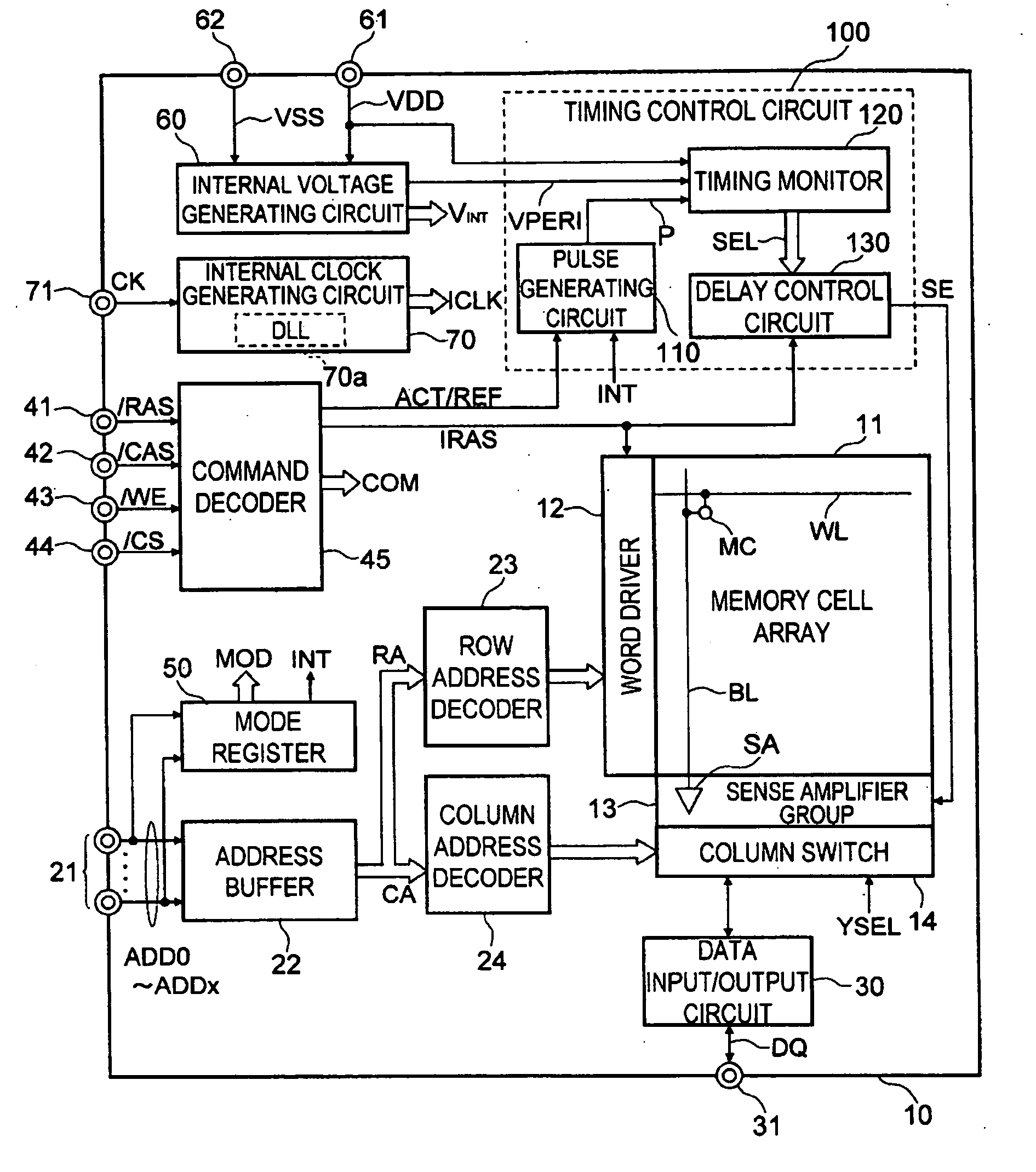
[0026]FIG. 1 is a block diagram showing a configuration of a semiconductor device 10 according to an embodiment of the present invention.

[0027]The semiconductor device 10 according to the first embodiment includes a memory cell array 11 that includes a plurality of word lines WL, a plurality of bit lines BL, and a plurality of memory cells MC each arranged at a point at the intersection of the word line WL with the bit line BL. For simplicity, one word line WL, one bit line BL, and one memory cell MC are shown in FIG. 1. The memory cell MC used in the present embodiment is a DRAM, although it is not particularly limited thereto.

[0028]The word lines WL are connected to a word driver 12, and any one of the word lines WL is selected by the word driver 12. The selection of the word line WL by the word driver 12 is performed based on a row address RA supplied...


PUM


Abstract

A first delay circuit and a second delay circuit having different operation conditions from each other, a detection circuit that detects a difference in propagation speed of a pulse signal, which is simultaneously input to the first and second delay circuits, and a setting circuit that generates a selection signal based on a detection result from the detection circuit are provided. The selection signal is supplied to a delay control circuit that generates an operation timing signal by delaying a reference signal, of which a delay amount is controlled by the selection signal. With this arrangement, a necessity to set the delay amount of the delay control circuit with a large design margin can be eliminated considering PVT variation, and as a result, performance degradation can be prevented.

Description

BACKGROUND OF THE INVENTION[0001]1. Field of the Invention[0002]The present invention relates to a semiconductor device, and, more particularly relates to a semiconductor device including a delay control circuit that generates an operation timing signal by delaying a reference signal.[0003]2. Description of Related Art[0004]An internal circuit of a semiconductor device generally uses a clock signal to determine its operation timing. Therefore, it suffices to increase a frequency of the clock signal to operate the semiconductor device at high speed.[0005]However, in a semiconductor memory device such as a DRAM (Dynamic Random Access Memory), increasing a frequency of a clock signal cannot always lead to a high speed operation of its memory cell array because the memory cell array performs an analog operation. Consequently, an interval from a timing for starting a predetermined operation (for example, an activation timing of a word driver) for the memory cell array to another timing f...

Claims


Application Information

Patent Timeline
IPC IPC(8): G11C7/00H03L7/06G11C11/4076H03K5/00H03K5/13H03K5/26
CPCG11C7/22G11C11/4076G11C7/222
Inventor NAGATA, KYOICHI
Owner LONGITUDE LICENSING LTD
Why Eureka
Try Eureka