Modulation Circuit and Semiconductor Device Including the Same

Inactive Publication Date: 2010-04-08
SEMICON ENERGY LAB CO LTD
View PDF52 Cites 5 Cited by
  • Summary
  • Abstract
  • Description
  • Claims
  • Application Information

AI Technical Summary

Benefits of technology

[0025]According to one embodiment of the present invention, the generation of a reverse current in a modulation circuit can be prevented, resulting in a reduction in the power consumption of the modulation circuit. The reduction in the power consumption of the modulation circuit mak

Problems solved by technology

Although an ideal modulation circuit should operate in the aforementioned manner, it is difficult that a modulation circuit actually manufactured operates in the aforementioned manner, and the following problems occur.
This reverse curre

Method used


Image

  • Modulation Circuit and Semiconductor Device Including the Same
  • Modulation Circuit and Semiconductor Device Including the Same
  • Modulation Circuit and Semiconductor Device Including the Same

Examples


embodiment 1

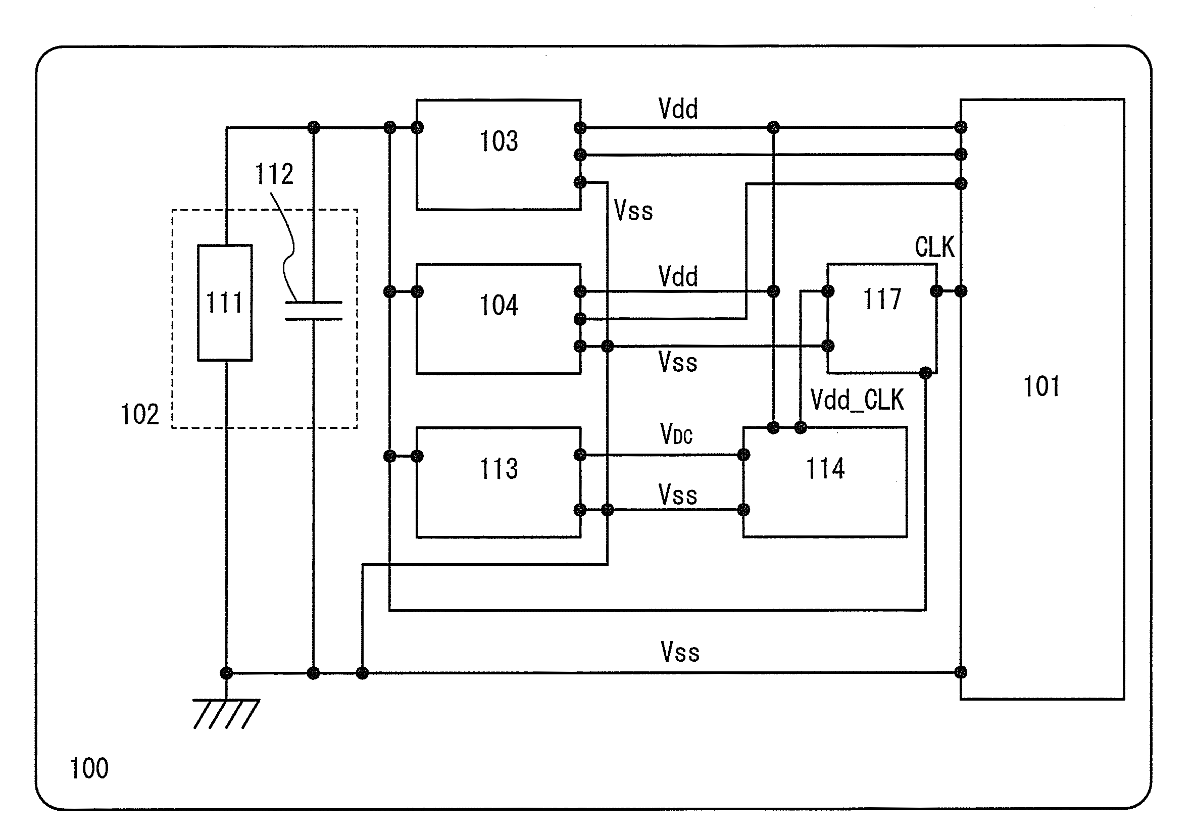
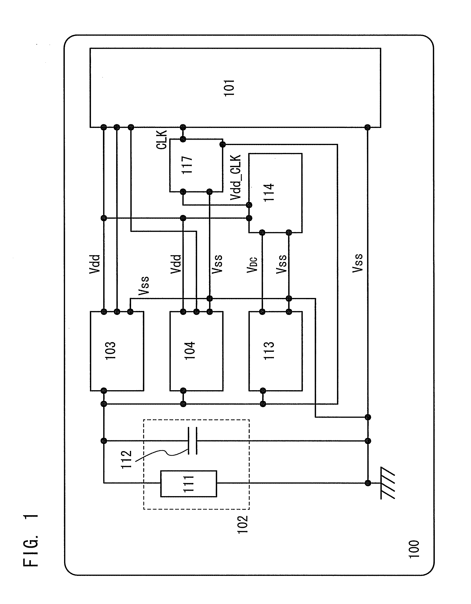
[0041]FIG. 1 is a block diagram illustrating the whole RF tag used as one embodiment of the present invention. An RF tag 100 includes: a logic circuit 101 for carrying out functional processing such as generation of a response signal in accordance with received data; an antenna circuit 102 for transmitting and receiving (communicating) signals to and from a reader / writer; a demodulation circuit 103 for demodulating an amplitude-modulated wave (a wave obtained by overlapping a carrier wave with a modulated wave) received by the antenna circuit 102 to extract a pulsed signal; a modulation circuit 104 for modulating a carrier wave output from the reader / writer in accordance with a response signal output from the logic circuit 101 and transmitting a response signal to the reader / writer; a rectifier circuit 113 for generating a DC voltage from a carrier wave or an amplitude modulated wave received by the antenna circuit 102; a constant voltage circuit 114 for converting a DC voltage gene...

embodiment 2

[0050]In this embodiment, a configuration and operation of the modulation circuit shown in Embodiment 1 will be described in detail. FIGS. 3A and 3B illustrate an example of a circuit configuration of the modulation circuit of one embodiment of the present invention.

[0051]First, a configuration of the modulation circuit of this embodiment will be described with reference to FIG. 3A. A modulation circuit 300 employs a load switching method and includes a load 301, a diode 302, and a switch 303. An anode (one terminal) of the diode 302 is electrically connected to one terminal of an antenna 304 via the load 301; a cathode (the other terminal) of the diode 302 is electrically connected to one terminal of the switch 303; and the other terminal of the switch 303 is electrically connected to the other terminal of the antenna 304.

[0052]Note that the antenna described in this specification is a balanced device; therefore, a sine wave with a certain frequency is input to each of the two term...

embodiment 3

[0064]This embodiment shows another configuration of the modulation circuit described in Embodiment 2, in which a resistor is used as the load 301; a diode-connected transistor is used as the diode 302; and a transistor is used as the switch 303. Note that a diode-connected n-channel transistor is used as the diode 302 in this embodiment; however, the polarity of the diode-connected transistor is not limited as described in Embodiment 2. Furthermore, an n-channel transistor is used as the switch 303 in this embodiment; however, the polarity of the transistor is not limited as described in Embodiment 2.

[0065]FIG. 4A illustrates a circuit configuration of the modulation circuit of this embodiment. A modulation circuit 400 employs a load switching method and includes a resistor 401, a diode-connected n-channel transistor 402 (hereinafter, referred to as a diode-connected transistor 402), and a transistor 403. One of a source and a drain of the diode-connected transistor 402 and a gate ...


PUM


Abstract

An object of the present invention is to reduce the power consumption of a modulation circuit. The modulation circuit includes a load, a diode, and a transistor. An anode of the diode is electrically connected to one terminal of an antenna via the load; a cathode of the diode is electrically connected to one of a source and a drain of the transistor; the other of the source and the drain of the transistor is electrically connected to the other terminal of the antenna; and the transistor is controlled to be turned on or off in accordance with a signal input to a gate of the transistor.

Description

TECHNICAL FIELD[0001]The invention disclosed in this specification relates to a semiconductor device (a data carrier) capable of wirelessly communicating (transmitting / receiving) data. In particular, the present invention relates to a modulation circuit using a load switching method.BACKGROUND ART[0002]In recent years, individual identification technologies have attracted attention. In these technologies, Identification information is assigned to each object to recognize the history of information on the object and to be utilized in production, management, or the like. In particular, RFID (radio frequency identification) technologies for transmitting and receiving data through wireless communication have been developed in the market. A wireless communication system using RFID technologies is constituted by a wireless communication device (an interrogator) and a data carrier (a transponder), and data is wirelessly communicated between them. The wireless communication device means a d...

Claims


Application Information

Patent Timeline
IPC IPC(8): H04M1/00H04B1/38G06K19/07H01L21/822H01L27/04H03C1/14H04B1/02H04B5/02
CPCH04L27/04G06K19/0723
Inventor YAMASHITA, YUKIKONISHIJIMA, TATSUJI
Owner SEMICON ENERGY LAB CO LTD
Why Eureka
Try Eureka