
Composite type semiconductor device spacer sheet, semiconductor package using the same, composite type semiconductor device manufacturing method, and composite type semiconductor device

a semiconductor device and spacer technology, applied in the direction of printed circuit assembling, printed circuit manufacture, electrical apparatus construction details, etc., can solve the problems of reducing the thickness of the chip and the substrate, affecting the sealing of the conduction passage of the upper semiconductor package with the mother board, and causing shortening between adjacent connection terminals. achieve the effect of high packaging density

Inactive Publication Date: 2010-04-15
LINTEC CORP
View PDF2 Cites 28 Cited by
  • Summary
  • Abstract
  • Description
  • Claims
  • Application Information

AI Technical Summary

Benefits of technology

[0013]According to the present invention, a wiring and connecting method by a spacer sheet which satisfies securement of a height of a connection terminal distance and a narrow pitch thereof at the same time in a POP type semiconductor package has been able to be provided, and this has made it possible to provide a complex type semiconductor device of a POP type having a high packaging density.

Problems solved by technology

In contrast with this, in combination of grid terminal type semiconductor packages themselves such as BGA (ball grid array) and the like, not only terminals arranged on a lower surface interrupt connection of the semiconductor packages, but also the problem that it is difficult to secure a conduction passage of an upper semiconductor package with a mother board is involved therein.
However, if a connection terminal is increased in a size under an existing situation in which a pitch between connection terminals has to be narrowed by an increase in pins, short between adjacent connection terminals themselves is caused.
Further, a decrease in the thicknesses of a chip and a substrate brings about an increase in the cost to a large extent.

Method used


Image

  • Composite type semiconductor device spacer sheet, semiconductor package using the same, composite type semiconductor device manufacturing method, and composite type semiconductor device
  • Composite type semiconductor device spacer sheet, semiconductor package using the same, composite type semiconductor device manufacturing method, and composite type semiconductor device
  • Composite type semiconductor device spacer sheet, semiconductor package using the same, composite type semiconductor device manufacturing method, and composite type semiconductor device

Examples


example 1

[0119]a) The adhesive layer δ was applied on one surface of the base material layer α (50 μm) so that a thickness thereof after dried was 40 μm, and then it was dried at 90° C. for 2 minutes. Thereafter, the release film α was stuck on an exposed surface of the adhesive layer to prepare a sheet on which the base material layer α / the adhesive layer δ / the release film α were laminated.

[0120]Further, the adhesive layer δ was applied on one surface of another base material layer α so that a thickness thereof after dried was 40 μm, and it was dried at 90° C. for 2 minutes. Then, a base material layer face of the sheet described above was stuck on an exposed surface of the adhesive layer immediately after dried to obtain a sheet material [A] for a spacer sheet. The sheet material [A] assumed, as shown in FIG. 6, a five-layer structure described later and had a thickness of 180 μm excluding that of the release film α.

Layer structure: base material layer α (50 μm) / adhesive layer δ (40 μm) / b...

example 2

[0121]A diameter of a lead-free solder for the upper BGA semiconductor package in Example 1 was changed from a diameter of 450 μm in Example 1 to a diameter of 300 μm, and a diameter of a lead-free solder for the lower BGA semiconductor package was changed from a diameter of 250 μm in Example 1 to a diameter of 450 μm. Further, the step g) was carried out in advance before the step e), and then the same procedure as in Example 1 was carried out, except that in the step e), the respective through holes and the space part in the spacer sheet [A] were opposed to the substrate of the upper BGA semiconductor package and fitted to the positions of the electrodes of the above substrate and the position of the principal part of the lower semiconductor package and that the above respective through holes were inserted into the connection terminals of the substrate in the upper BGA semiconductor package to stick them. Possibility of electrical connection and a distance between the upper and lo...

example 3

[0122]The adhesive layer β was applied on one surface of the base material layer β so that a thickness thereof after dried was 55 μm, and then it was dried at 130° C. for 3 minutes. Thereafter, the release film β was stuck on an exposed surface of the adhesive layer to prepare a sheet material [B] (a thickness was 180 μm excluding that of the release film β) in which a layer structure was the base material layer β (125 μm) / the adhesive layer β (55 μm) / the release film β (38 μm) as shown in FIG. 5. Steps subsequent to the above step were the same as in Example 1. The step f) in Example 1 was excluded. A spacer sheet [B] was prepared from the sheet material [B]. Possibility of electrical connection and a distance between the upper and lower substrates in the complex type semiconductor device thus obtained were measured. The results thereof are shown in Table 1.


PUM


Abstract

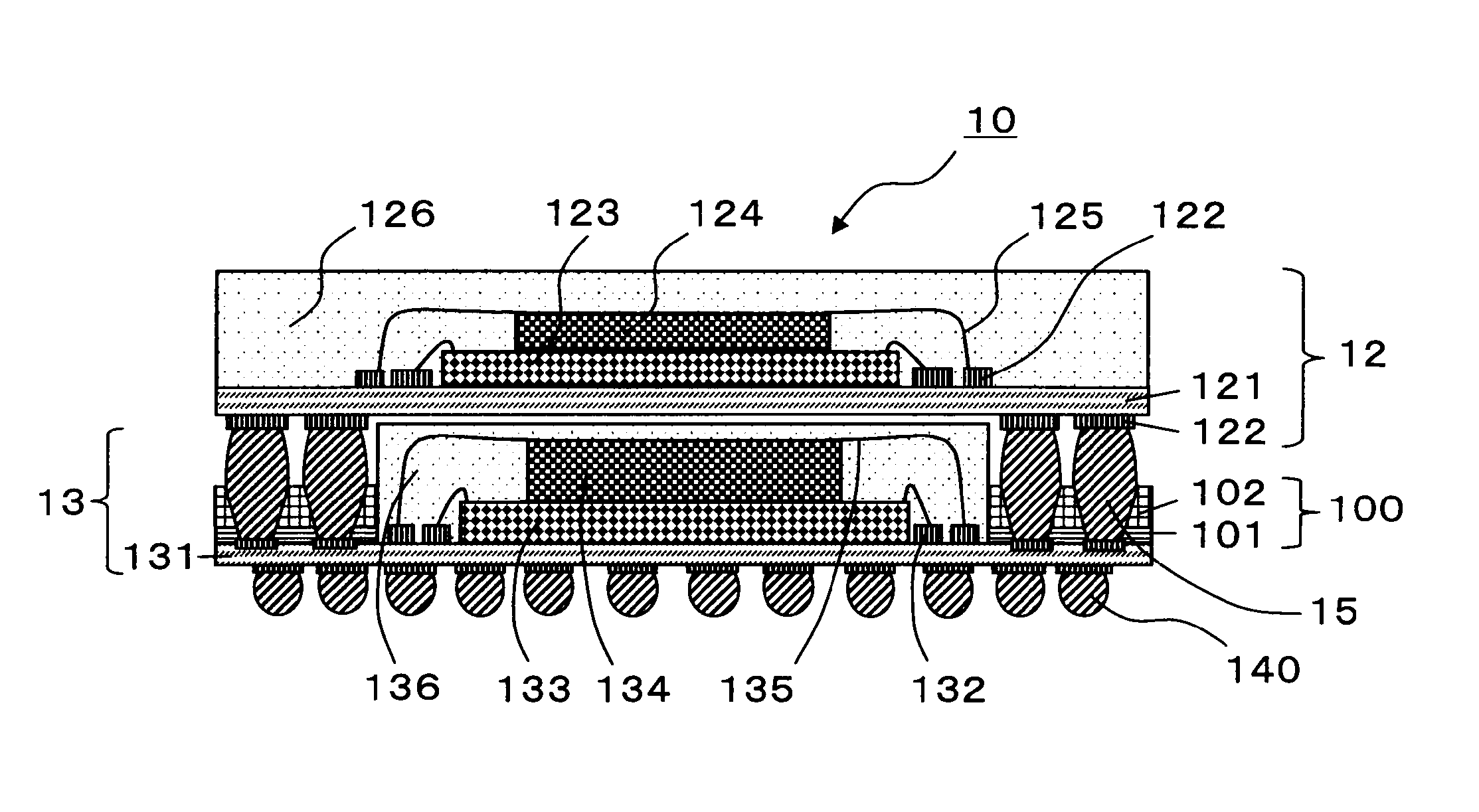
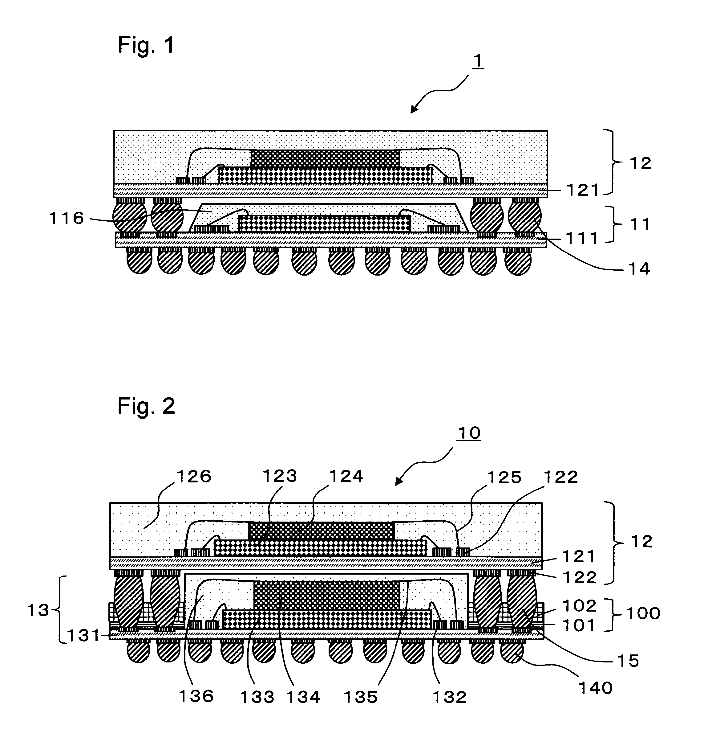
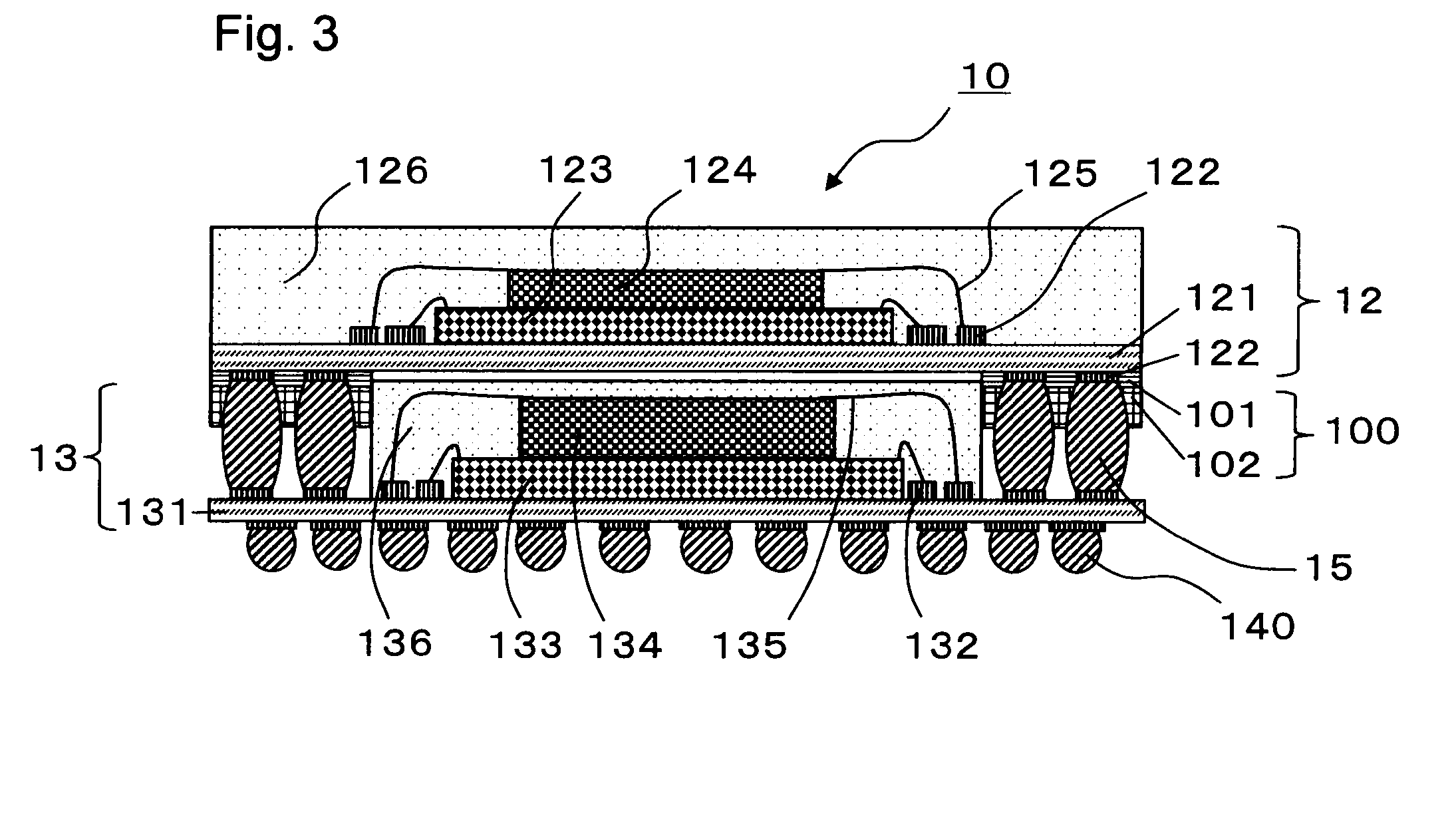
The present invention provides a spacer sheet for a complex type semiconductor device provided between the semiconductor packages of a complex type semiconductor device formed by laminating plural semiconductor packages, comprising through holes of an array corresponding to electrodes which can be provided onto a substrate of one semiconductor package and which are formed in order to connect and wire one semiconductor package with the other semiconductor package and a space part corresponding to a principal part of the above one semiconductor package mounted on the substrate or a principal part of the other semiconductor package opposed to the substrate and a production process for a complex type semiconductor device in which the above spacer sheet is used. It further provides a wiring and connecting method by using a spacer sheet which satisfies securing of a distance between connection terminals and a narrow pitch at the same time in a POP type semiconductor package and a complex type semiconductor device of a POP type which is increased in a packaging density by the above wiring and connecting method.

Description

BACKGROUND OF THE INVENTION[0001]The present invention relates to a spacer sheet disposed between semiconductor packages in order to secure conduction of a semiconductor package to an external electrode and an installation space of a semiconductor package in a complex type semiconductor device of a POP (package-on-package) type comprising combination of plural semiconductor packages, a semiconductor package prepared by using the same, a production process for a complex type semiconductor device and a complex type semiconductor device obtained by the above production process.RELATED ART[0002]In the semiconductor field, when a device is prepared by combining semiconductor chips having different circuits into one system, available are two techniques of SiP (system-in-package) in which another semiconductor chip is mounted on a semiconductor chip to obtain one package and POP in which plural semi-completed semiconductor chips are directly connected. SiP has the merits that since circuit...

Claims


Application Information

Patent Timeline
Patent Type & Authority Applications(United States)
IPC IPC(8): H01L23/52H05K7/00H01L21/60
CPCH01L25/0657H01L25/105H01L2924/15321H01L2224/48227H01L2225/1058H01L2225/1023H01L2224/73265H01L2224/32225H01L2224/32145H01L2224/16225H01L2924/01322H01L2924/01019H01L2924/15331H01L2924/1532H01L2924/15311H01L2924/01078H01L2924/01077H01L2225/06586H01L2225/06568H01L2225/0651H01L2224/73204H01L2224/48095H01L2224/48091H01L2224/16H01L2924/00014H01L2924/00012H01L2924/00H01L2924/181H01L24/73H01L2924/00011H01L2224/0401H01L23/02
Inventor SHINODA, TOMONORISHIZUHATA, HIRONORISHINODA, HIROFUMIKAWAMATA, YUJITASHIMA, TAKESHISHIMAMURA, MASATOWATANABE, MASAKOAMAGAI, MASAZUMI
Owner LINTEC CORP
Learn More