
Ceramic chip assembly

a chip assembly and ceramic technology, applied in resistor details, basic electric elements, solid-state devices, etc., can solve the problems of shock and friction, electrical performance may easily be deteriorated, and limitations in the related field, and achieve the effect of thin thickness

Inactive Publication Date: 2010-04-15
JOINSET
View PDF37 Cites 17 Cited by
  • Summary
  • Abstract
  • Description
  • Claims
  • Application Information

AI Technical Summary

Benefits of technology

[0023]Another object of the present invention is to provide a ceramic chip assembly protecting damages from external loads, shocks, and frictions.
[0031]A further another object of the present invention is to provide a ceramic chip assembly, where a lead wire is easily inserted into a PCB to be soldered, has little tendency to be returned by elasticity to be easily secured at a certain part, and is not easily cut off by a repeated force.

Problems solved by technology

In this case, because ceramic chips having the electrical characteristics of semiconductors have so weak mechanical strength that they may be fragile by external loads, shocks and frictions and their electrical performance may easily be deteriorated by the external environmental changes such as humidity, an insulating substance is coated on the ceramic chip and the connection region between the ceramic chip and the lead wire after the lead wire is soldered to the ceramic chip.
However, there are the following limitations in the related-art.
Also, this is not suitable for a ceramic bare chip having lightweight and slim profile.
However, a related-art structure of the ceramic chip assembly is difficult to satisfy these characteristics.
However, according to the modified structure, the price of the lead frame is more expensive than cylindrical metal lead wire, and continuous production in reel taping manner is difficult.
The thickness of a ceramic bare chip or a ceramic chip that is inserted between the lead frames is thicker than the lead frame, so that a protruded part thereof may be easily broken or damaged by external loads, shocks, or frictions.
That is, since the lead frame has a relatively thin thickness, the lead frame has a limitation in physically protecting the ceramic bare chip or the ceramic chip from horizontal or vertical shocks or frictions.
On the other hand, even when the thickness part of the lead frame is upright in a width direction so as to contact with the ceramic bare chip 10 or the ceramic chip, it is difficult to protect the ceramic chip from external load, shocks, or frictions that are exerted along the vertical direction of the ceramic chip assembly.
Thus, the area occupied by the soldered part is so small that the soldering strength may be weak.
In addiction, since the structure of the lead frame has a rectangular shape, it is inefficient to insert the lead frame into a circular hole of the PDB for soldering.
Since the thin plate lead frame has a tendency to be recovered by its elasticity until being completely bent, the lead frame is difficult to fix at a certain spot.
Furthermore, since a hot melt adhesive is melted by heat, the adhesive strength may be significantly reduced at a high temperature, making it difficult to protect the ceramic chip.
Moreover, the ceramic chip applied to the lead frame is a ceramic bare chip having a mono-layer of a thin thickness that does not include an internal electrode foamed therein, making it difficult to provide a ceramic chip assembly having various performances.

Method used


Image

  • Ceramic chip assembly
  • Ceramic chip assembly
  • Ceramic chip assembly

Examples


Embodiment Construction

[0057]Now, preferred embodiments of the present invention will be described in detail with reference to the accompanying drawings.

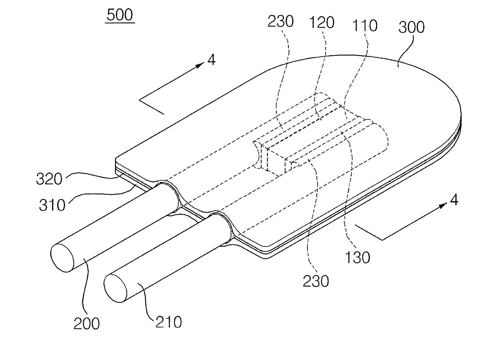
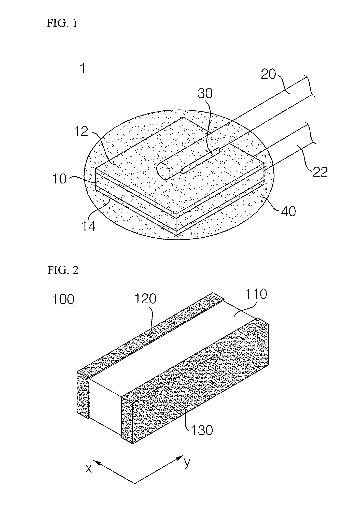
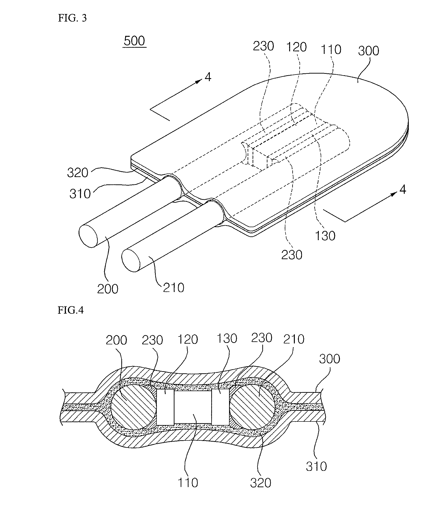
[0058]FIG. 2 is a view illustrating an exemplary ceramic chip 100 applied to a ceramic chip assembly according to an embodiment.

[0059]Referring to FIG. 2, the ceramic chip 100 includes a ceramic base 110 and external electrodes 120 and 130.

[0060]The ceramic base 110 has a hexahedral shape and electrical characteristics.

[0061]The external electrodes 120 and 130 are oppositely formed on both side surfaces of the ceramic base 110.

[0062]According to an embodiment, the size, the thickness, and the width of the ceramic chip 100 may be about 1 mm, about 0.30 mm, and about 0.5 mm, respectively, but is not limited thereto.

[0063]If the size of the ceramic chip 100 is too small, the automation by a real taping may be difficult when the ceramic chip assembly is manufactured.

[0064]The external electrodes 120 and 130 may be formed on both ends of the ceramic base 110 i...


PUM


Abstract

A ceramic chip assembly is provided. The ceramic chip assembly includes a ceramic base, a plurality of external electrodes, a pair of cylindrical metal lead wires, and an insulating protection material. The ceramic base has electrical characteristics of a semiconductor. The pair of external electrodes is oppositely formed on both side surfaces of the ceramic base, respectively. The cylindrical metal lead wire has one end thereof electrically and mechanically connected to the external electrodes by an electrical conductive adhesive, respectively, and has an external diameter identical to or greater than the thickness of the ceramic base. The insulating protection material includes a pair of insulating films and an insulating coating layer.

Description

BACKGROUND ART[0001]1. Field of the Invention[0002]The present invention relates to a ceramic chip assembly, and more particularly, to a ceramic chip assembly having a thin thickness and improved mechanical strength, which includes an insulating protection layer having a uniform thickness. Also, the present invention relates to a ceramic chip assembly, an internal ceramic chip of which is protected from external loads, shocks and frictions, and nearly not influenced by external environment. Furthermore, the present invention relates to a ceramic chip assembly having high productive and economical efficiency because its material cost is cheap and continuous job is possible in reel taping manner.[0003]2. Description of the Related Art[0004]As a method of mounting a ceramic chip having electrical characteristics of semiconductors such as thermistors, magnetic substances, and piezoelectrics onto a printed circuit board (PCB), there is a method of electrically and mechanically connecting...

Claims


Application Information

Patent Timeline
IPC IPC(8): H01L23/48H01L21/60H01L41/39
CPCH01C1/028H01C1/148H01L41/08H01L2224/4918H01L41/0533H01L41/23H01L41/29H01L41/0475H10N30/883H10N30/875H10N30/02H10N30/06
Inventor KIM, SUN-KILEE, SUK-JOO
Owner JOINSET
Learn More