Semiconductor device and method of fabricating the same

a semiconductor and device technology, applied in semiconductor devices, digital storage, instruments, etc., can solve the problems of small saturated current of medium voltage devices, difficult chip reduction, poor performance, etc., and achieve the effect of higher saturated current and better performan

Active Publication Date: 2010-04-22
UNITED MICROELECTRONICS CORP
View PDF3 Cites 43 Cited by
  • Summary
  • Abstract
  • Description
  • Claims
  • Application Information

AI Technical Summary

Benefits of technology

[0007]The present invention provides a semiconductor device including a high voltage device, a medium voltage device and a low voltage device formed on a single chip. The ...

Problems solved by technology

However, during the operation, the saturated current of the medium voltage device is small and the performance of the same is bad.
Further, the occupied chip area bec...

Method used


Image

  • Semiconductor device and method of fabricating the same
  • Semiconductor device and method of fabricating the same
  • Semiconductor device and method of fabricating the same

Examples


Embodiment Construction

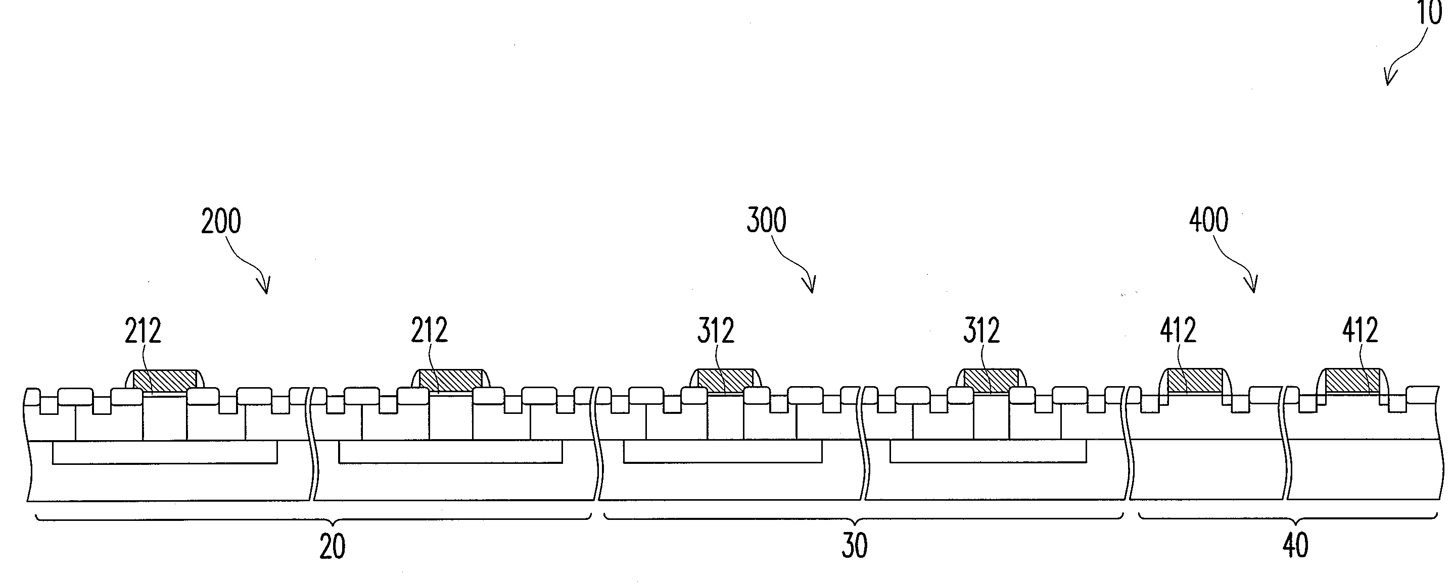
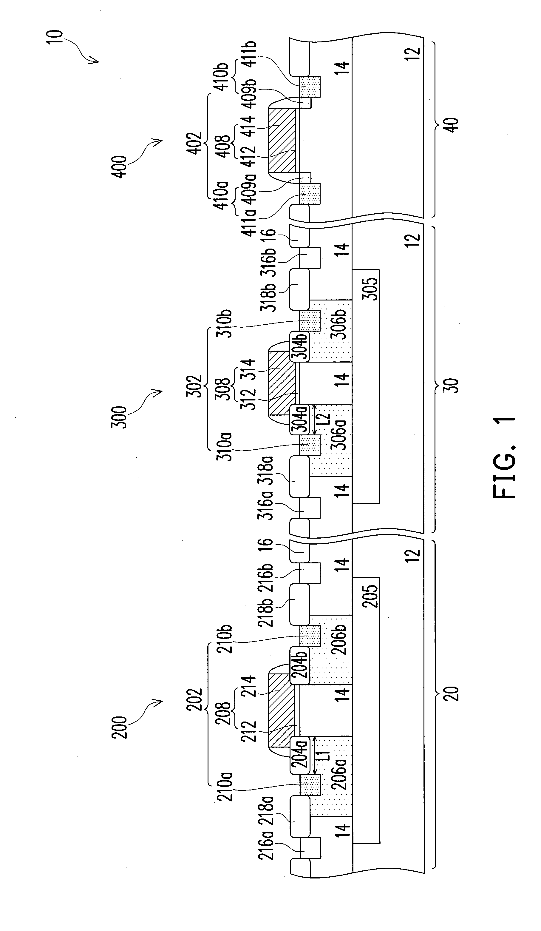
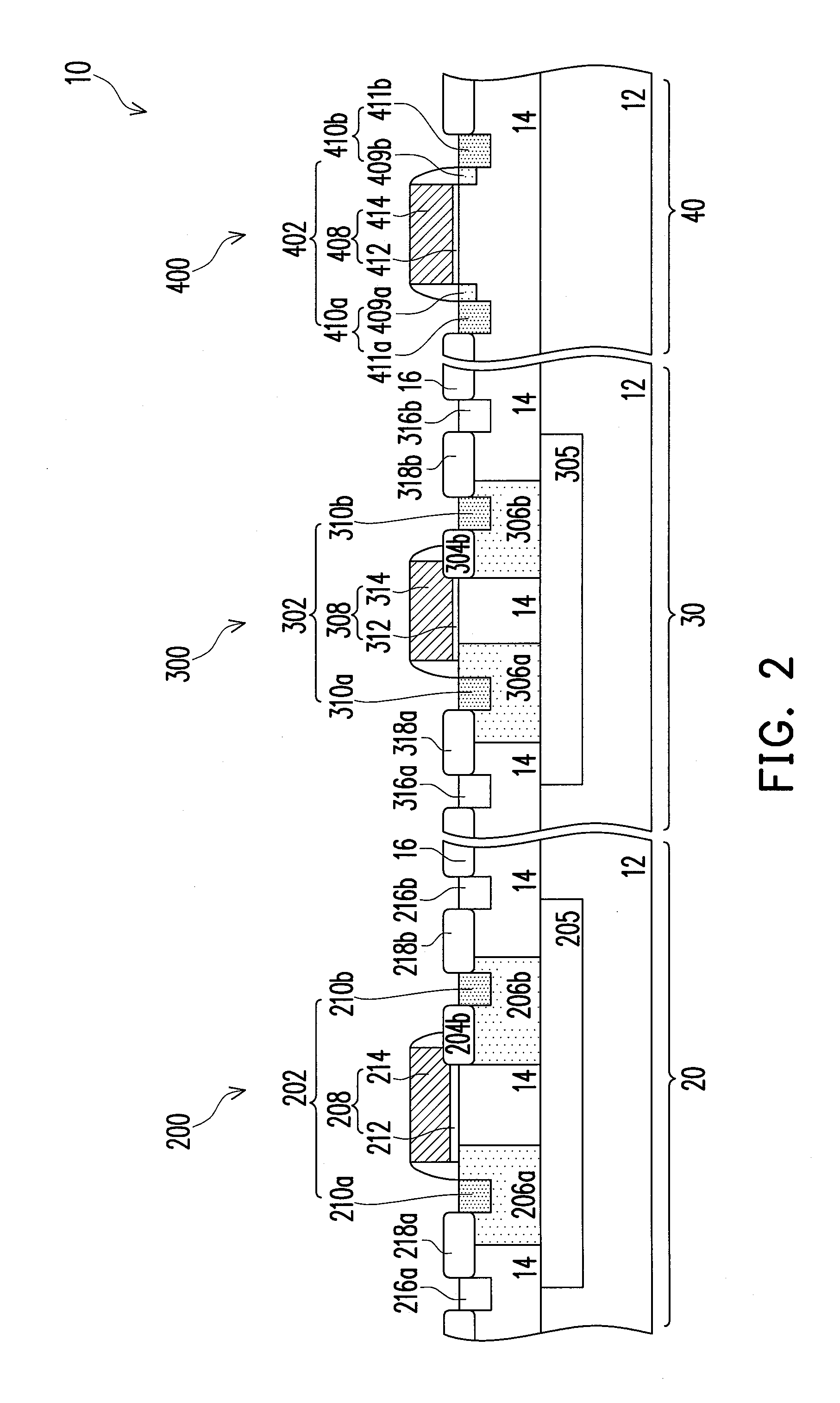
[0037]FIG. 1 schematically illustrates a cross-section view of a semiconductor device according to an embodiment of the present invention.

[0038]Referring to FIG. 1, a semiconductor device 10 of the present invention includes a substrate 12 of a first conductivity type or a substrate 12 having a first well 14 of a first conductivity type therein, a high voltage device 200 of a second conductivity type, a medium voltage device 300 of the second conductivity type and a low voltage device 400 of the second conductivity type. In the following embodiments, the present invention is illustrated by a substrate 12 having a first well 14 of a first conductivity type. The first conductivity type is different from the second conductivity type. For example, the first conductivity is P-type and the second conductivity type is N-type, or the first conductivity type is N-type and the second conductivity type is P-type.

[0039]The substrate 12 includes a semiconductor material such as silicon. The subs...


PUM


Abstract

A semiconductor device including a substrate, a high voltage device, a medium voltage device and a low voltage device is provided. The substrate includes a high voltage circuit area, a medium voltage circuit area and a low voltage circuit area. The high voltage device, the medium voltage device and the low voltage device are respectively disposed in the high voltage circuit area, the medium voltage circuit area and the low voltage circuit area. The medium voltage device and the high voltage device have the same structure while the medium voltage device and the low voltage device have different structures. Further, the high voltage device, the medium voltage device and the low voltage device respectively include a first gate dielectric layer, a second gate dielectric layer and a third gate dielectric layer, and the thickness of the second gate dielectric layer is smaller than that of the first gate dielectric layer.

Description

BACKGROUND OF THE INVENTION[0001]1. Field of Invention[0002]The present invention relates to an integrated circuit and a method of fabricating the same, and more generally to a semiconductor device and a method of fabricating the same.[0003]2. Description of Related Art[0004]Multi-function products with light weights, slim shapes and small sizes have become the mainstream in the market as the technology is developed. Accordingly, the operation voltage of the internal circuit of a single technology product is reduced, and the number and types of circuits or integrated circuit chips are required more.[0005]Generally, the voltage level shift among integrated circuits with different voltage levels is performed through a voltage level shift circuit. A typical voltage level shift circuit usually receives the signal of an IC internal device from a low voltage device, passes the signal through a medium voltage device and then a high voltage device, and outputs the signal from the high volta...

Claims


Application Information

Patent Timeline
IPC IPC(8): H01L27/092H01L27/088H01L21/8238
CPCH01L21/823814H01L21/823878H01L21/823857
Inventor CHEN, CHIN-LUNGHUANG, HAN-MIN
Owner UNITED MICROELECTRONICS CORP
Why Eureka
Try Eureka