
Semiconductor package, semiconductor module, and method for fabricating the semiconductor package

a semiconductor module and semiconductor technology, applied in the field of semiconductor devices, can solve the problems of complicated process for forming semiconductor chips or external terminals, and achieve the effect of simplifying the fabrication process and reliably forming the sam

Inactive Publication Date: 2010-04-22
SAMSUNG ELECTRONICS CO LTD
View PDF11 Cites 58 Cited by
  • Summary
  • Abstract
  • Description
  • Claims
  • Application Information

AI Technical Summary

Benefits of technology

[0006]Example embodiments provide a semiconductor package and a method for fabricating the same reliably while simplifying a fabrication process.
[0007]Example embodiments also provide a semiconductor package having a simpler structure and a method for fabricating the same.

Problems solved by technology

In a stage for fabricating the chip scale package or the wafer level package, however, a process for forming semiconductor chips or external terminals may be complicated.

Method used


Image

  • Semiconductor package, semiconductor module, and method for fabricating the semiconductor package
  • Semiconductor package, semiconductor module, and method for fabricating the semiconductor package
  • Semiconductor package, semiconductor module, and method for fabricating the semiconductor package

Examples


Embodiment Construction

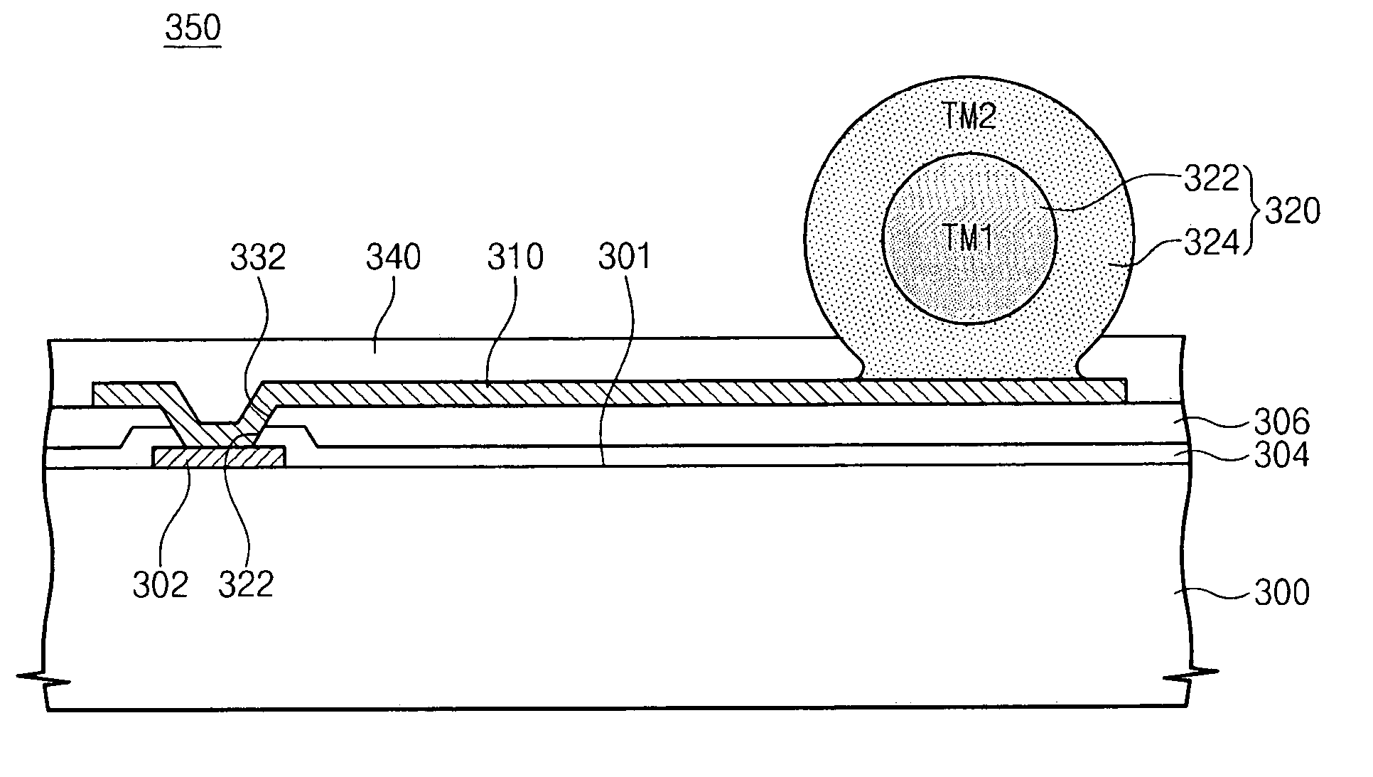
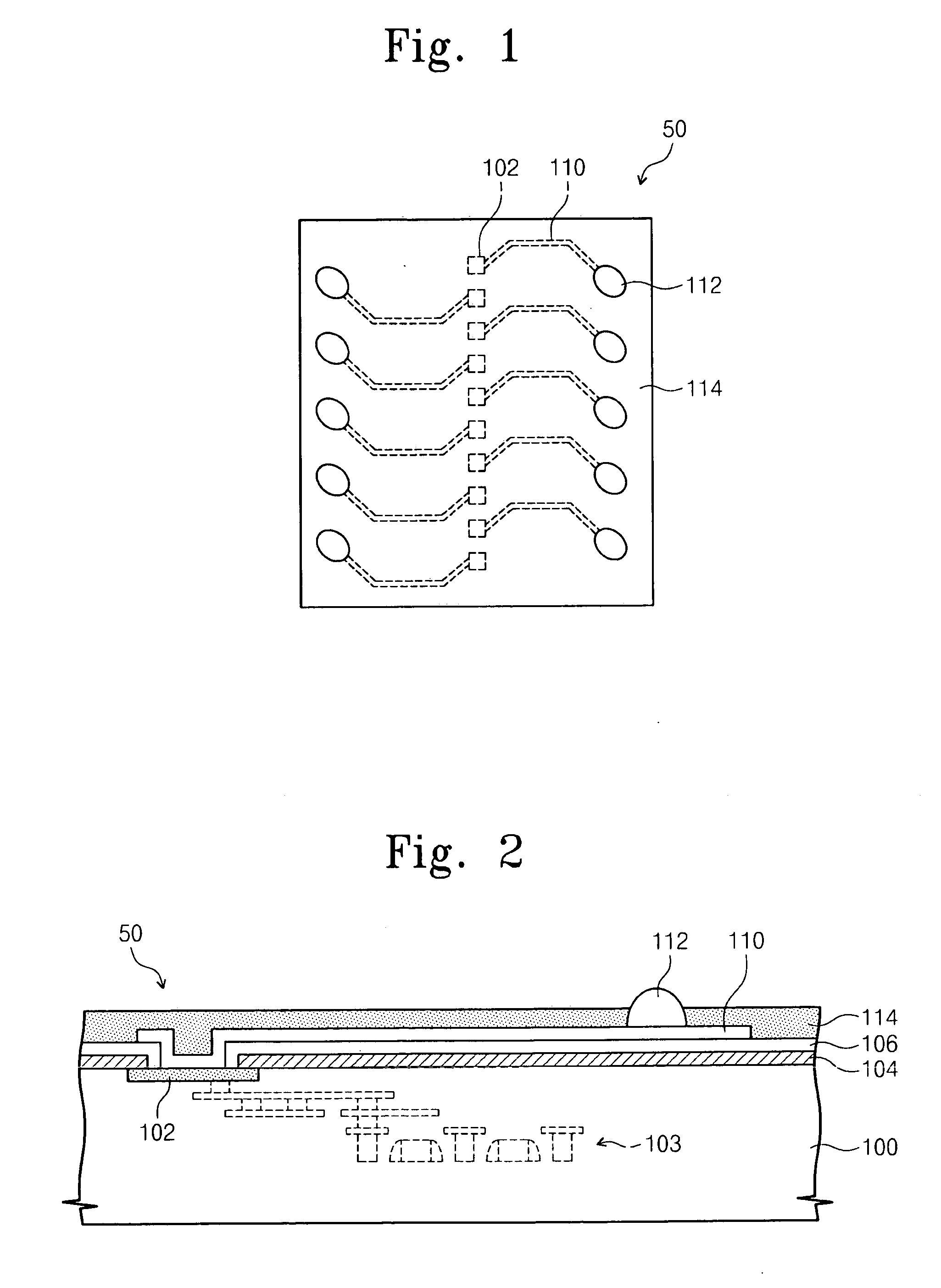
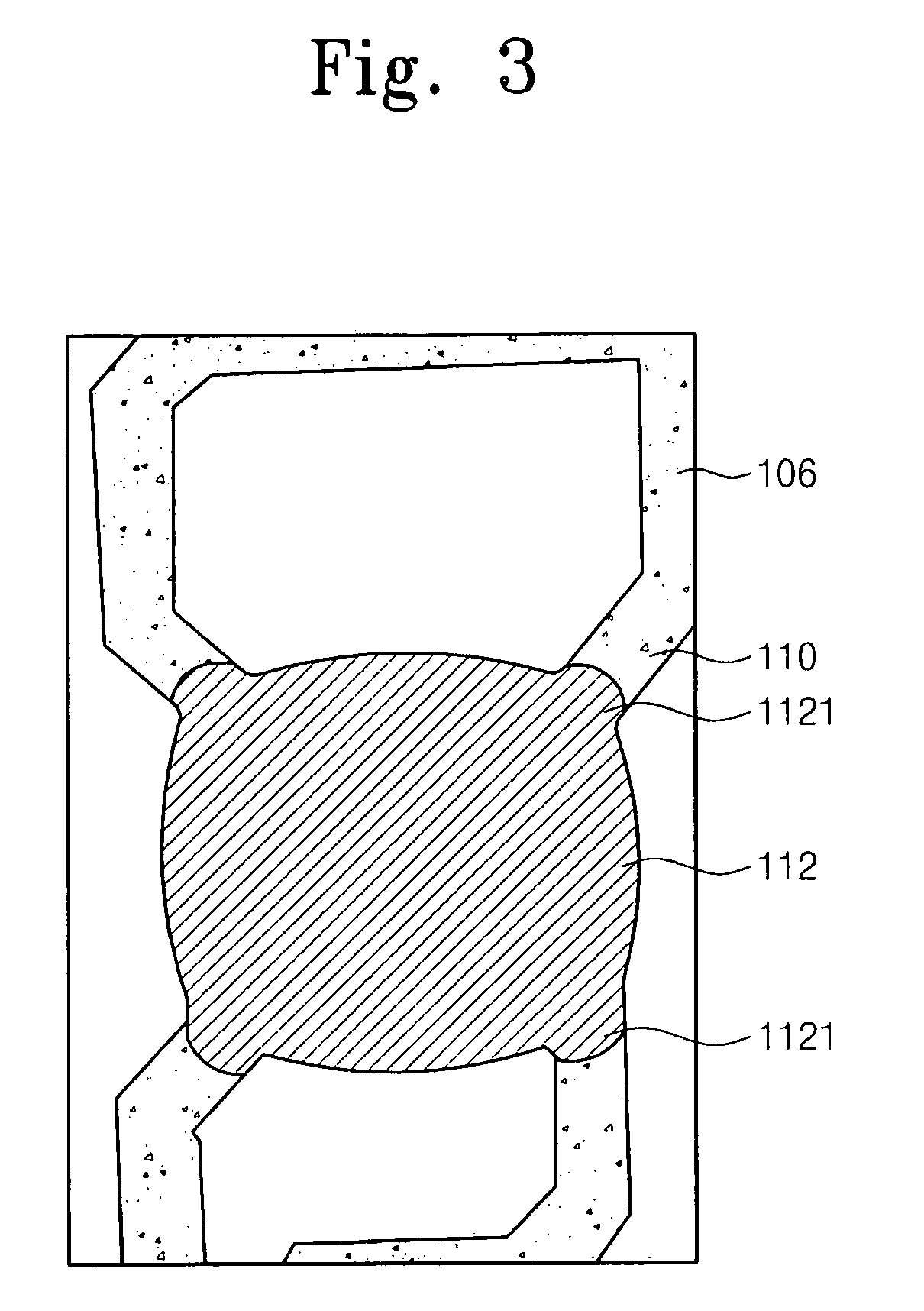
[0057]Example embodiments will be described below in more detail with reference to the accompanying drawings. Example embodiments may, however, be embodied in different forms and should not be construed as limited to example embodiments set forth herein. Rather, example embodiments are provided so that this disclosure will be thorough and complete. In the figures, the dimensions of elements may be exaggerated for clarity of illustration.

[0058]It will be understood that although the terms first and second are used herein to describe various elements, these elements should not be limited by these terms. These terms are only used to distinguish one element from another element.

[0059]The advantages, features and aspects of example embodiments will become apparent from the following description with reference to the accompanying drawings, which is set forth hereinafter. Example embodiments may, however, be embodied in different forms and should not be construed as limited to the embodime...


PUM


Abstract

Provided is a semiconductor package, a semiconductor module and a method for fabricating the semiconductor package. The method provides a substrate including a bonding pad. The method forms a dielectric layer for exposing the bonding pad on the substrate. The method forms a redistribution line which is electrically connected to the bonding pad, on the dielectric layer. The method forms an external terminal which is electrically connected to the bonding pad without using a solder mask which limits a position of the external terminal, on the redistribution line.

Description

CROSS-REFERENCE TO RELATED APPLICATIONS[0001]This application claims priority under 35 U.S.C. §119 to Korean Patent Application No. 10-2008-0102145, filed on Oct. 17, 2008, Korean Patent Application No. 10-2008-0109862, filed on Nov. 6, 2008, and Korean Patent Application No. 10-2009-0049948, filed on Jun. 5, 2009, the entire contents of each are hereby incorporated by reference in their entirety.BACKGROUND[0002]1. Field[0003]Example embodiments herein relate to a semiconductor device, and more particularly, to a semiconductor package, a semiconductor module and a method for fabricating the semiconductor package.[0004]2. Description of the Related Art[0005]In the semiconductor industry, techniques for miniaturizing and lightening semiconductor devices are being researched. In the conventional art, a package technology, called Chip Scale Package (CSP) or chip size package in which the size of semiconductor package is miniaturized to the size of the semiconductor chip level, is being ...

Claims


Application Information

Patent Timeline
IPC IPC(8): H01L23/498H01L21/768
CPCH01L21/568H01L23/3114H01L23/525H01L24/06H01L24/11H01L24/13H01L2224/0231H01L2224/02313H01L2224/0401H01L2224/04042H01L2224/06136H01L2224/111H01L2224/1191H01L2224/13012H01L2224/13022H01L2224/13099H01L2924/01013H01L2924/01014H01L2924/01029H01L2924/0103H01L2924/01042H01L2924/01047H01L2924/0105H01L2924/01073H01L2924/01074H01L2924/01078H01L2924/01079H01L2924/01082H01L2924/014H01L2924/14H01L2224/11334H01L2924/01005H01L2924/01006H01L2924/01033H01L2924/01041H01L2224/0233H01L2224/0239H01L2224/13147H01L2224/13155H01L2224/13609H01L2224/13611H01L2924/0001H01L2224/13014H01L2924/00014H01L2924/01083H01L2924/00012H01L2924/181H01L2924/00
Inventor LEE, JONGGIKANG, SUNWONKIM, YOUNG LYONGLEE, JONGHOJANG, CHUL-YONGKIM, MINILLAHN, EUNCHULLEE, KWANG YONGBAEK, SEUNGDUKHONG, JI-SEOK
Owner SAMSUNG ELECTRONICS CO LTD
Features
  • Generate Ideas
  • Intellectual Property
  • Life Sciences
  • Materials
  • Tech Scout
  • Unparalleled Data Quality
  • Higher Quality Content
  • 60% Fewer Hallucinations
Learn More