
Eureka
For R&D, Eureka makes reading and utilizing patents & technical documents easy.
Eureka AIR
Designed for self-driven R&D workflows. Generate viable solutions, solve complex R&D challenges, empower your innovation with AI.

Eureka Materials
Designed for material experts only. Revolutionize your material R&D, from search, analyze, to developing new materials.

TechResearch
Generate reliable direction feasibility study reports for your R&D in just a few steps.

TechSeek
Discover and master advanced knowledge NOW. Basics, ideas, possibilities, all at once.

TechMind
As an expert in R&D Theories, TechMind can generates customized viable solutions instantly.

TechRisk
Analyze your overall solution with one click, know your potential R&D risks in advance.

TechMonitor
Get weekly tech updates, stay abreast of the latest tech innovations and key insights.
Plasma display panel
- Summary
- Abstract
- Description
- Claims
- Application Information
AI Technical Summary
Benefits of technology
Problems solved by technology
Method used
Image

Examples
first embodiment
[0069]A PDP of an embodiment according to the present invention was produced. Phosphors emitting three colors of red, green, and blue were prepared with the following materials: (Y,Gd)BO3:Eu as the main component of red phosphors, Zn2SiO4:Mn2+ as the main component of green phosphors, and BAM(BaMgAl10O17:Eu2+) as the main component of blue phosphors. However, the effect of the present invention is also effective when other materials are used as the main components of the respective phosphors of three colors.
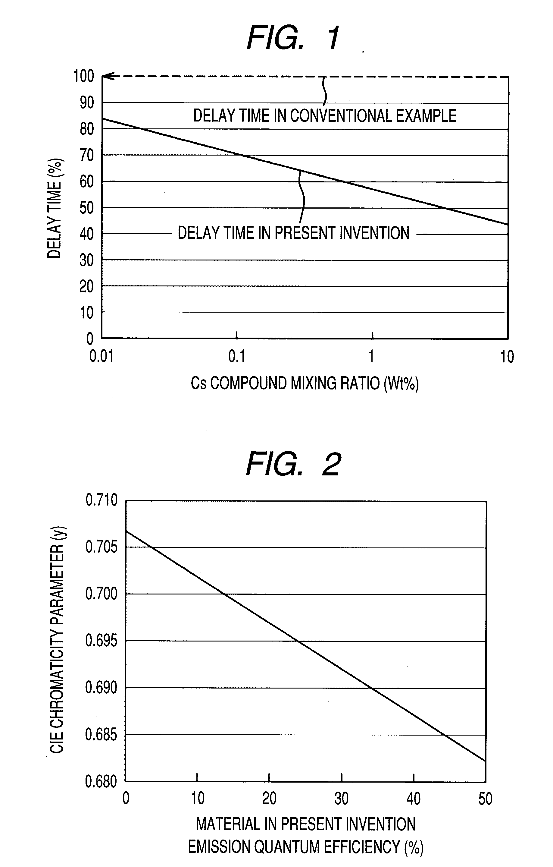
[0070]A display device according to the present invention was produced by mixing a predetermined amount of compound containing an element satisfying the conditions of the present invention, with respect to each of the phosphors of three colors. Examples of the compound satisfying the conditions include compounds represented by the following composition formulas: Cs(1−x)M1xAl02 (where M1 is the I group element, 0≦x(1−x)M2xAl(1+x)O(2+2x) (where M2 is the II group element, 0≦x100 sh...
second embodiment
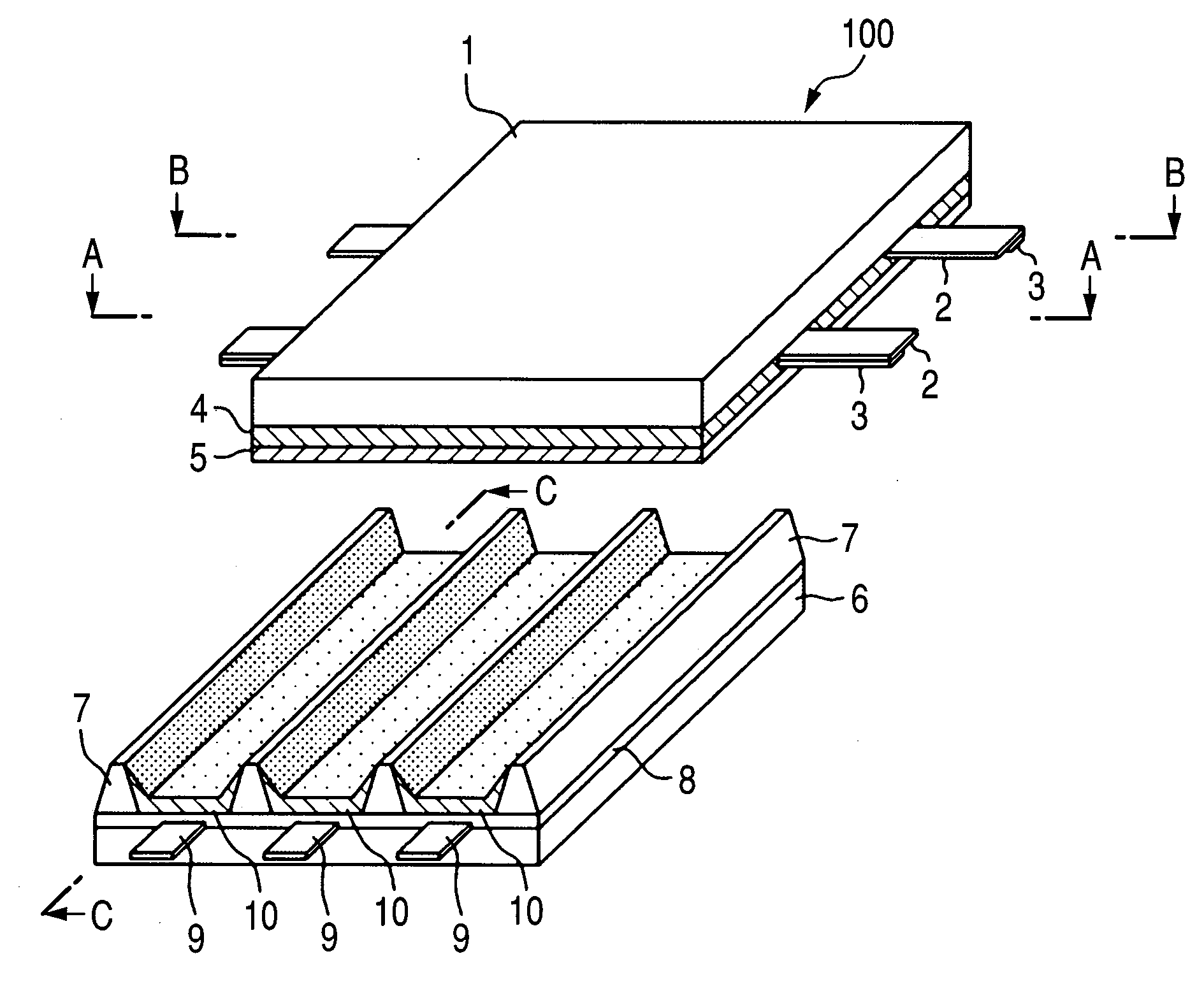
[0084]A PDP of a second embodiment according to the present invention was produced. The basic structure, phosphor materials, and production method are the same as those in the first embodiment. The second embodiment is different from the first embodiment in that the compound 12 containing the element satisfying the conditions of the present invention is not mixed in each of the red, green, and blue phosphors for performing image display. In this embodiment, a display device according to the present invention was produced by forming a predetermined amount of the compound 12 according to the present invention in at least a portion of a surface of the dielectric layer 8, the top and side surfaces of the barrier ribs 7.
[0085]A specific example of the production method is as follows. That is, as shown in FIG. 10, before the formation of the phosphor layers 10, a layer of a predetermined amount of the material 12 according to the present invention is formed in the top and side surfaces of...
third embodiment
[0088]A PDP of a third embodiment according to the present invention was produced. The basic structure, phosphor material, and production method are the same as those in the first embodiment.
[0089]The third embodiment is different from the first embodiment in that the compound 12 containing the element satisfying the conditions of the present invention is not mixed in each of the red, green, and blue phosphors for performing image display. As shown in FIG. 12, a display device according to the present invention was produced by forming the compound 12 according to the present invention as a thin film at least in a portion on the side of the substrate 1, namely, on a surface of the protective layer. FIG. 12 is a schematic cross-sectional view of a case in which the material 12 according to the present invention is applied to the surface of the protective layer of the substrate 1 by evaporation or sputtering.
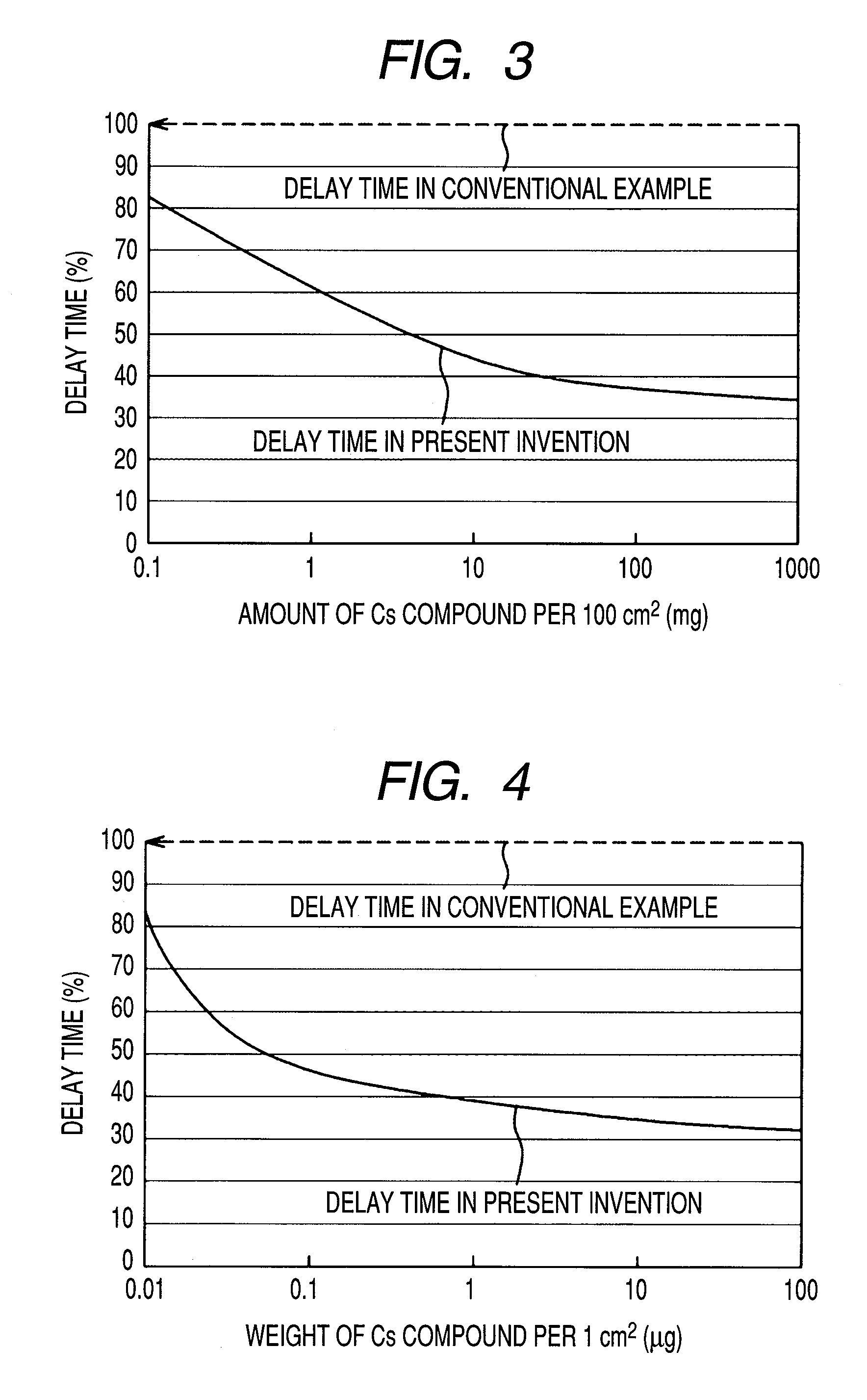
[0090]FIG. 4 is a graph showing the effect of reducing the discharge delay tim...
PUM
 Abstract
Description
Claims
Application Information
 - R&D Engineer
- R&D Manager
- IP Professional
- Industry Leading Data Capabilities
- Powerful AI technology
- Patent DNA Extraction
Browse by: Latest US Patents, China's latest patents, Technical Efficacy Thesaurus, Application Domain, Technology Topic, Popular Technical Reports.
© 2024 PatSnap. All rights reserved.Legal|Privacy policy|Modern Slavery Act Transparency Statement|Sitemap|About US| Contact US: help@patsnap.com