
Plasma display panel and manufacturing method thereof

A technology of a plasma display screen and a manufacturing method, which is applied to the field of plasma display screen and manufacturing, can solve the problems of increasing the number of lines, reducing the discharge space, and failing to meet the quality requirements of the full high-definition PDP display screen.

Inactive Publication Date: 2012-03-07
SICHUAN COC DISPLAY DEVICES
View PDF3 Cites 0 Cited by
  • Summary
  • Abstract
  • Description
  • Claims
  • Application Information

AI Technical Summary

Problems solved by technology

[0004] However, with the emergence of full high-definition televisions, the pixel pitch of the PDP display is getting smaller and smaller, which directly affects the discharge space and brightness of the screen. The effect achieved by covering a protective layer of magnesium oxide on the dielectric layer can no longer meet the quality requirements of full high-definition PDP displays

Method used

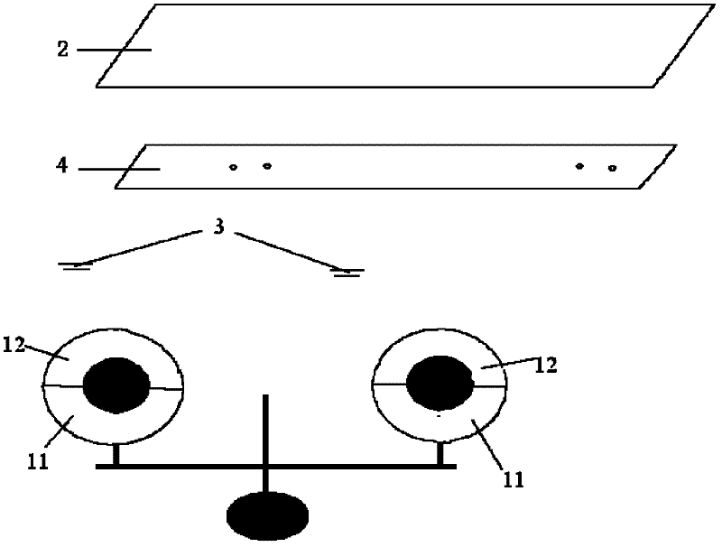
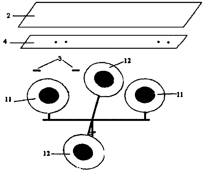
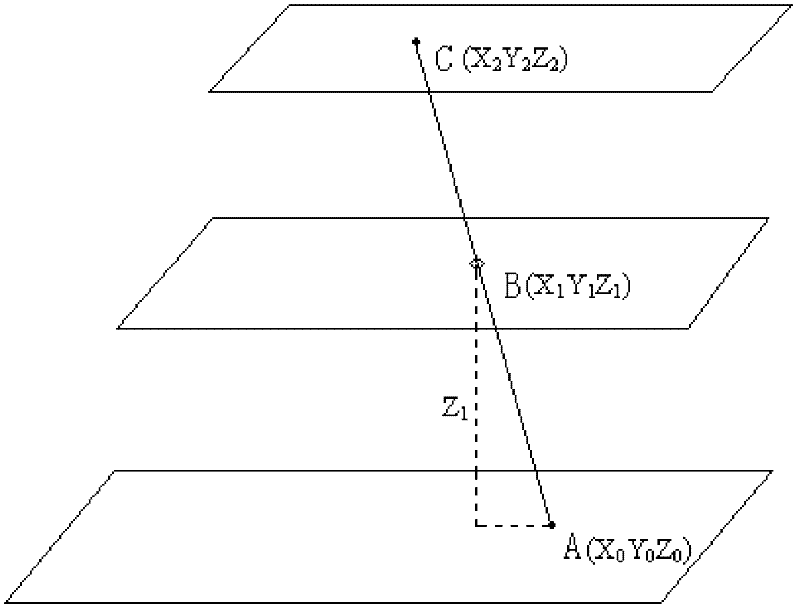

Image

  • Plasma display panel and manufacturing method thereof
  • Plasma display panel and manufacturing method thereof
  • Plasma display panel and manufacturing method thereof

Examples


Embodiment 1

[0040] Embodiment 1 technological step

[0041] The pre-order steps are the same as those of the prior art, and the process steps for forming the second protective layer: firstly, vacuum the chamber so that the degree of vacuum is 1.9×10 -4 Pa, the temperature was raised to 290°C while evacuating; after that, oxygen was passed into the chamber to reduce the vacuum to 2.8×10 -2 Pa, and then steam to reduce the vacuum to 5.1×10 -2 Pa; keep the moving speed of the substrate at 420 mm / sec during evaporation; finally control the thickness of the second protective layer to be 3700 angstroms.

Embodiment 2

[0042] Embodiment 2 technological steps

[0043] The steps are the same as in Example 1, the difference is: first vacuumize the chamber so that the degree of vacuum is 5.0×10 -4 Pa, the temperature was raised to 300°C while evacuating.

Embodiment 3

[0044] Embodiment 3 technological steps

[0045] The steps are the same as in Example 1, the difference is: first vacuumize the chamber so that the degree of vacuum is 7.6 × 10 -4 Pa, the temperature was raised to 310°C while evacuating.


PUM

PropertyMeasurementUnit
thicknessaaaaaaaaaa
thicknessaaaaaaaaaa
thicknessaaaaaaaaaa

Abstract

The invention discloses a plasma display panel and a manufacturing method of a protective layer. The display panel comprises an upper substrate and a lower substrate, wherein the upper substrate and the lower substrate are sealed oppositely. A discharge electrode, a dielectric layer and a protective layer are successively arranged on the upper substrate; and the protective layer includes: a first protective layer, which is formed by magnesium oxide; and a second protective layer, which is covered on the first protective layer; besides, the second protective layer consists of alkaline earth oxide and silica / titanium dioxide. According to a technical scheme provided in the invention, a second protective layer is evaporated and plated on a magnesium oxide film layer, so that a few doping atoms are mixed in a crystal structure of the magnesium oxide; after the doping atoms replace atoms in the magnesium oxide, a diffusion coefficient of the crystal is increased, so that the diffusion coefficient of the crystal structure containing the doping atoms is greater than a self-diffusion coefficient of a crystal only having a single atom; and therefore, an electron motion speed is accelerated and the electronic number is increased; an emission coefficient of a secondary electron is increased; a working voltage of a plasma display panel (PDP) is reduced; and discharge delay time is further reduced.

Description

technical field [0001] The invention relates to the field of plasma display screens, in particular to a plasma display screen and a manufacturing method. Background technique [0002] Common AC gas discharge plasma display screens all adopt a surface discharge structure, which includes an upper substrate and a lower substrate sealed together with it. A transparent electrode ITO and a bus electrode are arranged on the upper substrate, and the transparent electrode and the bus electrode constitute a discharge electrode. The discharge electrode is further divided into a sustain discharge electrode X and a scan discharge electrode Y. The surface of the discharge electrode is covered with a dielectric layer, and the dielectric layer is covered with a protective layer. The protective layer is usually a magnesium oxide film. Addressing electrodes perpendicular to the discharge electrodes are arranged on the lower substrate, and a layer of dielectric layer is covered on the address...

Claims


Application Information

Patent Timeline
Patent Type & Authority Applications(China)
IPC IPC(8): H01J1/70H01J17/49H01J9/20
Inventor 曹瑞林
Owner SICHUAN COC DISPLAY DEVICES
Learn More