Multi-level memory cell and manufacturing method thereof

a memory cell and multi-level technology, applied in semiconductor devices, digital storage, instruments, etc., can solve the problems of large increase in process complexity and cost, and the conventional rram cannot be used as a multi-level memory, so as to reduce the cost of multi-level memory cells, and reduce the difficulty of photolithography exposure.

Inactive Publication Date: 2010-04-29
IND TECH RES INST
View PDF9 Cites 9 Cited by
  • Summary
  • Abstract
  • Description
  • Claims
  • Application Information

AI Technical Summary

Benefits of technology

[0014]In a multi-level memory cell provided by the present invention, if spacers formed through a self-aligned process are served as dielectric layers for separating multiple memory material layers, steps in a photolithography process and the difficulty in photolithography exposure are reduced.
[0015]In a manufacturing method of a multi-level memory cell provided by the present invention, because spacers formed through a self-aligned process are served as dielectric layers for separating multiple memory material layers, steps in a photolithography process and the difficulty in photolithography exposure are reduced, and accordingly the cost of the multi-level memory cell is also reduced.

Problems solved by technology

However, the conventional RRAM cannot be served as a multi-level memory.
Additionally, because memory devices are made very small, the process complexity and cost thereof are greatly increased.

Method used


Image

  • Multi-level memory cell and manufacturing method thereof
  • Multi-level memory cell and manufacturing method thereof
  • Multi-level memory cell and manufacturing method thereof

Examples


Embodiment Construction

[0020]Reference will now be made in detail to the present preferred embodiments of the invention, examples of which are illustrated in the accompanying drawings. Wherever possible, the same reference numbers are used in the drawings and the description to refer to the same or like parts.

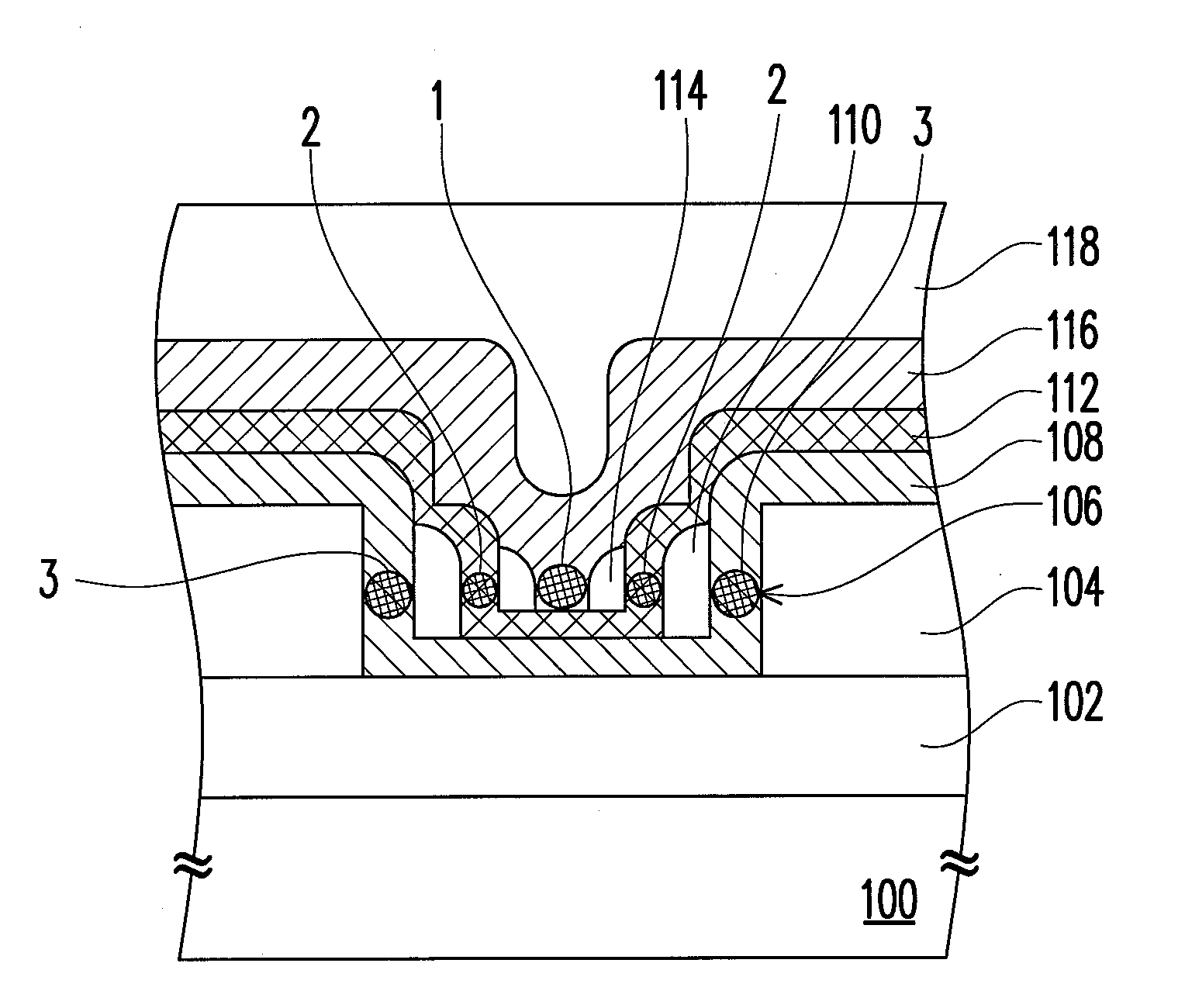
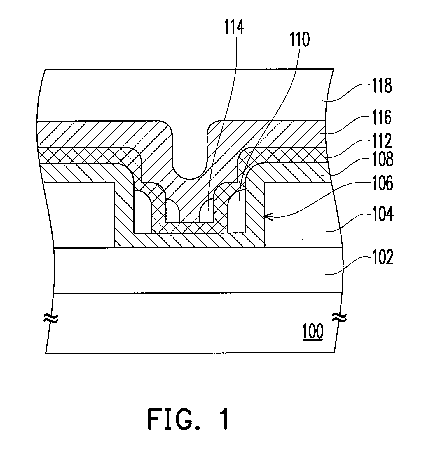
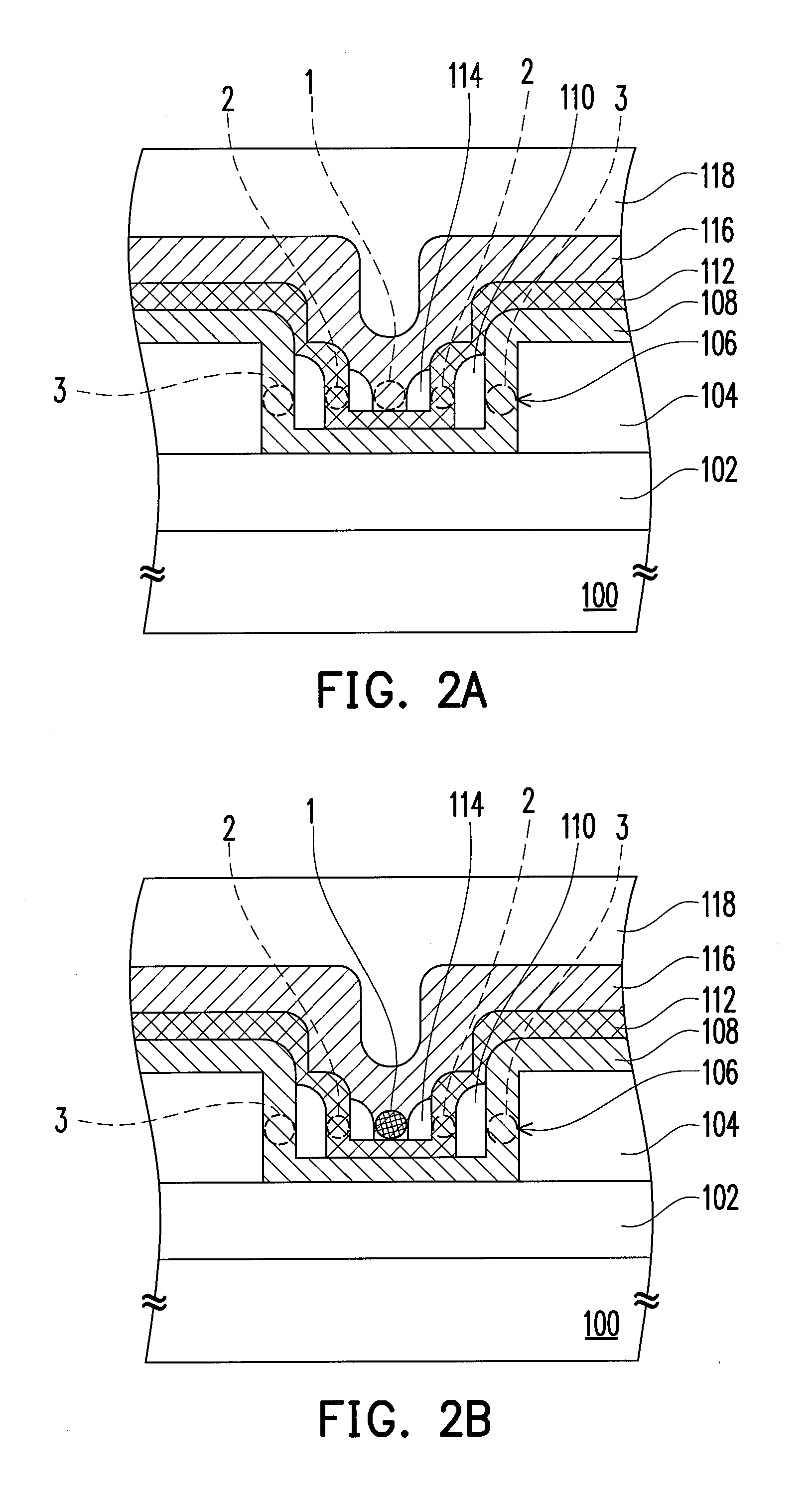
[0021]The present invention provides a multi-level memory cell which includes a lower electrode, a first dielectric layer, a plurality of memory material layers, a plurality of second dielectric layers, and an upper electrode. The lower electrode is disposed in the substrate. The first dielectric layer is disposed on the substrate and has an opening which exposes the lower electrode. The memory material layers are stacked on a sidewall of the first dielectric layer exposed by the opening and are electrically connected to the lower electrode. The second dielectric layers are respectively disposed between every adjacent two of the memory material layers and are located on the sidewall of the first diel...


PUM


Abstract

A multi-level memory cell having a bottom electrode, a first dielectric layer, a plurality of memory material layers, a plurality of second dielectric layers, and an upper electrode is provided. The bottom electrode is disposed in a substrate. The first dielectric layer is disposed on the substrate and has an opening exposing the bottom electrode. The memory material layers are stacked on a sidewall of the first dielectric layer exposed by the opening and are electrically connected to the bottom electrode. The second dielectric layers are respectively disposed between every adjacent two memory material layers and are located on the sidewall of the first dielectric layer. The upper electrode is disposed on the memory material layers. A manufacturing method of the multi-level memory cell is further provided. A multi-bit data can be stored in a single memory cell, and both the process complexity and the cost are reduced.

Description

CROSS-REFERENCE TO RELATED APPLICATION[0001]This application claims the priority benefit of Taiwan application serial no. 97140924, filed on Oct. 24, 2008. The entirety of the above-mentioned patent application is hereby incorporated by reference herein and made a part of specification.BACKGROUND OF THE INVENTION[0002]1. Field of the Invention[0003]The present invention generally relates to a semiconductor device, and more particularly, to a multi-level memory cell and a manufacturing method thereof.[0004]2. Description of Related Art[0005]Memory devices developed based on semiconductor techniques, such as dynamic random access memory (DRAM), static random access memory (SRAM), and non-volatile memory, have taken a major part in today's semiconductor industry. These memories have been broadly applied to personal computers, mobile phones, and networks and have become one of the most indispensable electronic products in our daily life.[0006]The demand to memories having low power cons...

Claims


Application Information

Patent Timeline
Patent Type & Authority Applications(United States)
IPC IPC(8): H01L29/18G11C11/00H01L21/02
CPCG11C11/5678G11C11/5685G11C13/0004H01L45/145G11C2213/32H01L45/04G11C13/0007H10N70/20H10N70/883
Inventor HSU, YEN-YACHEN, CHIH-WEI
Owner IND TECH RES INST
Why Eureka
Try Eureka