Methods of forming layers of semiconductor material having reduced lattice strain, semiconductor structures, devices and engineered substrates including same

a technology of semiconductor materials and lattice strain, applied in the direction of semiconductor devices, basic electric elements, electrical apparatus, etc., can solve the problems of increasing thickness, increasing lattice strain, and increasing thickness, so as to reduce the viscosity of the layer

Active Publication Date: 2010-05-06
S O I TEC SILICON ON INSULATOR THECHNOLOGIES
View PDF19 Cites 103 Cited by
  • Summary
  • Abstract
  • Description
  • Claims
  • Application Information

AI Technical Summary

Benefits of technology

[0016]In yet further embodiments, the present invention includes methods of forming engineered substrates. For example, an epitaxial layer of indium gallium nitride may be grown or otherwise formed on a substrate that includes a layer of glass material. A portion of the la...

Problems solved by technology

The formation and use of strained layers of semiconductor material is difficult because these strained layers may develop defects, such as dislocations, due to mismatch of the lattice parameters between adjacent materials.
However, as the concentration of dopant and the thickness of the layer of semiconductor material is increased, preserving a crystal structure having low-defect density becomes increasingly difficult.
Lattice strain is more problematic in indium gallium nitride device layers having higher indium content and increased thicknesses.
The presence of such lattice strain in a layer of semiconductor material may be undesirable for a number of reasons.
For example, the presence of lattice strain in a layer of semiconductor material may result in an increased density of defects (e.g., lattice dislocations) i...

Method used


Image

  • Methods of forming layers of semiconductor material having reduced lattice strain, semiconductor structures, devices and engineered substrates including same
  • Methods of forming layers of semiconductor material having reduced lattice strain, semiconductor structures, devices and engineered substrates including same
  • Methods of forming layers of semiconductor material having reduced lattice strain, semiconductor structures, devices and engineered substrates including same

Examples


Embodiment Construction

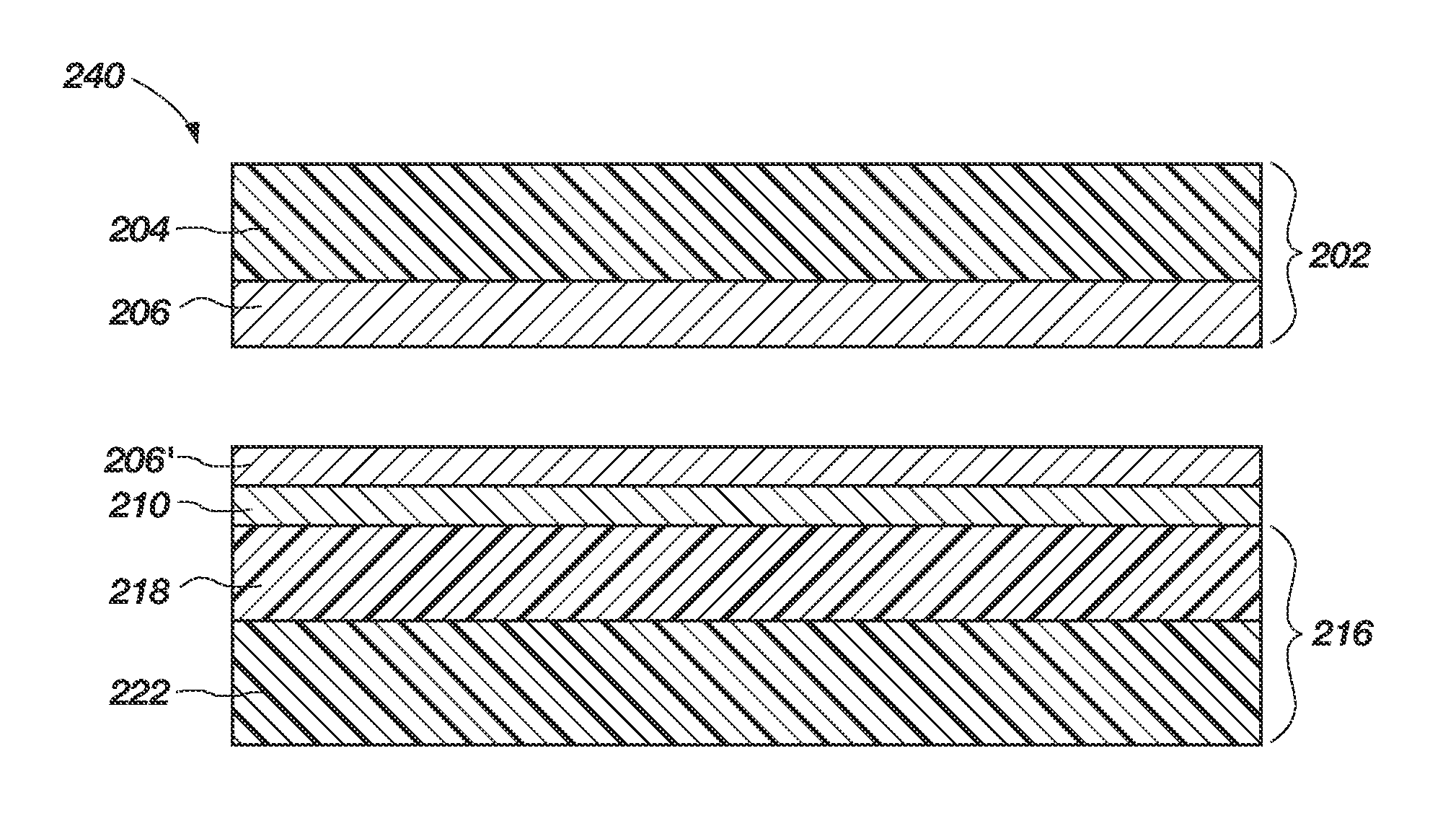
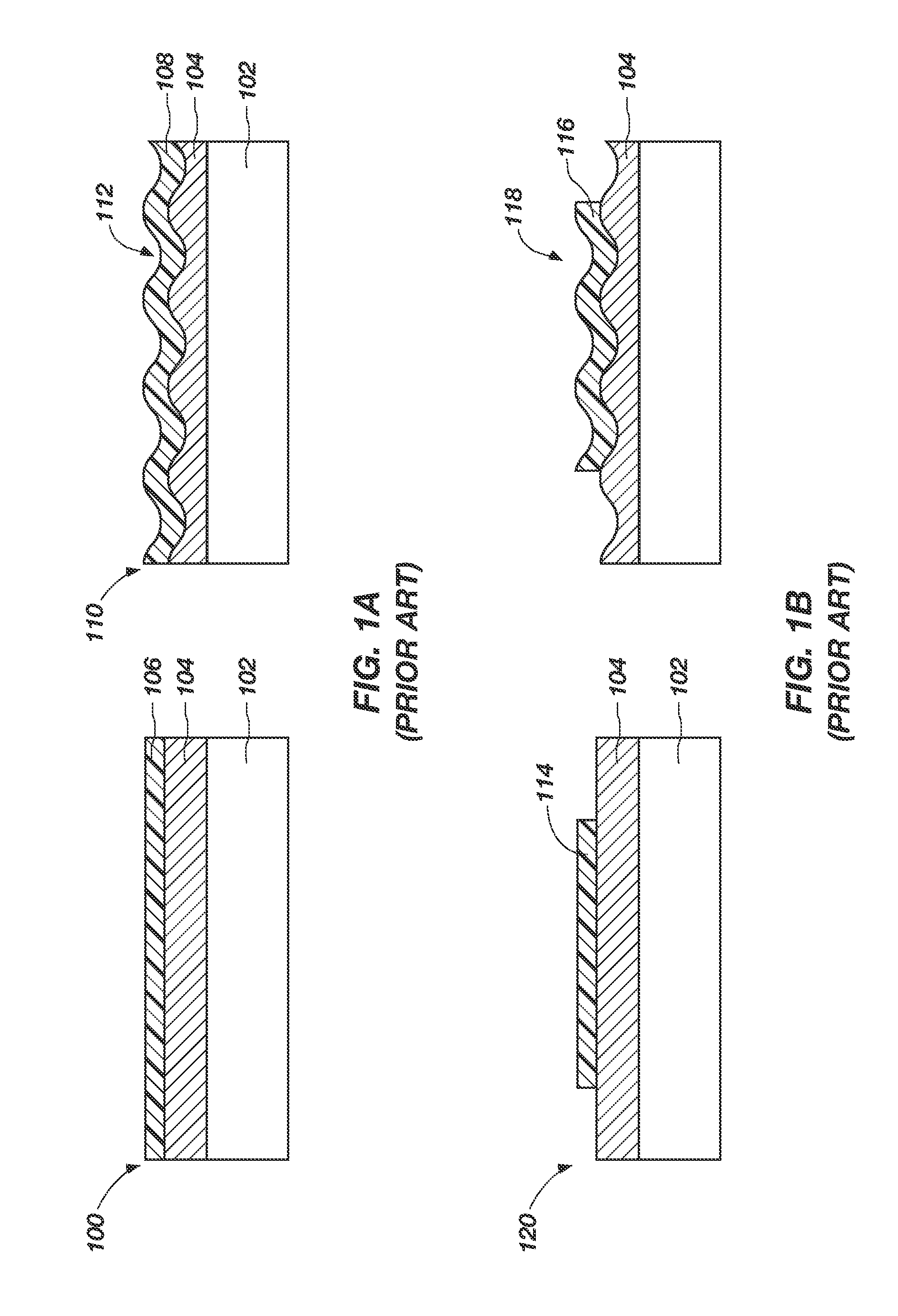
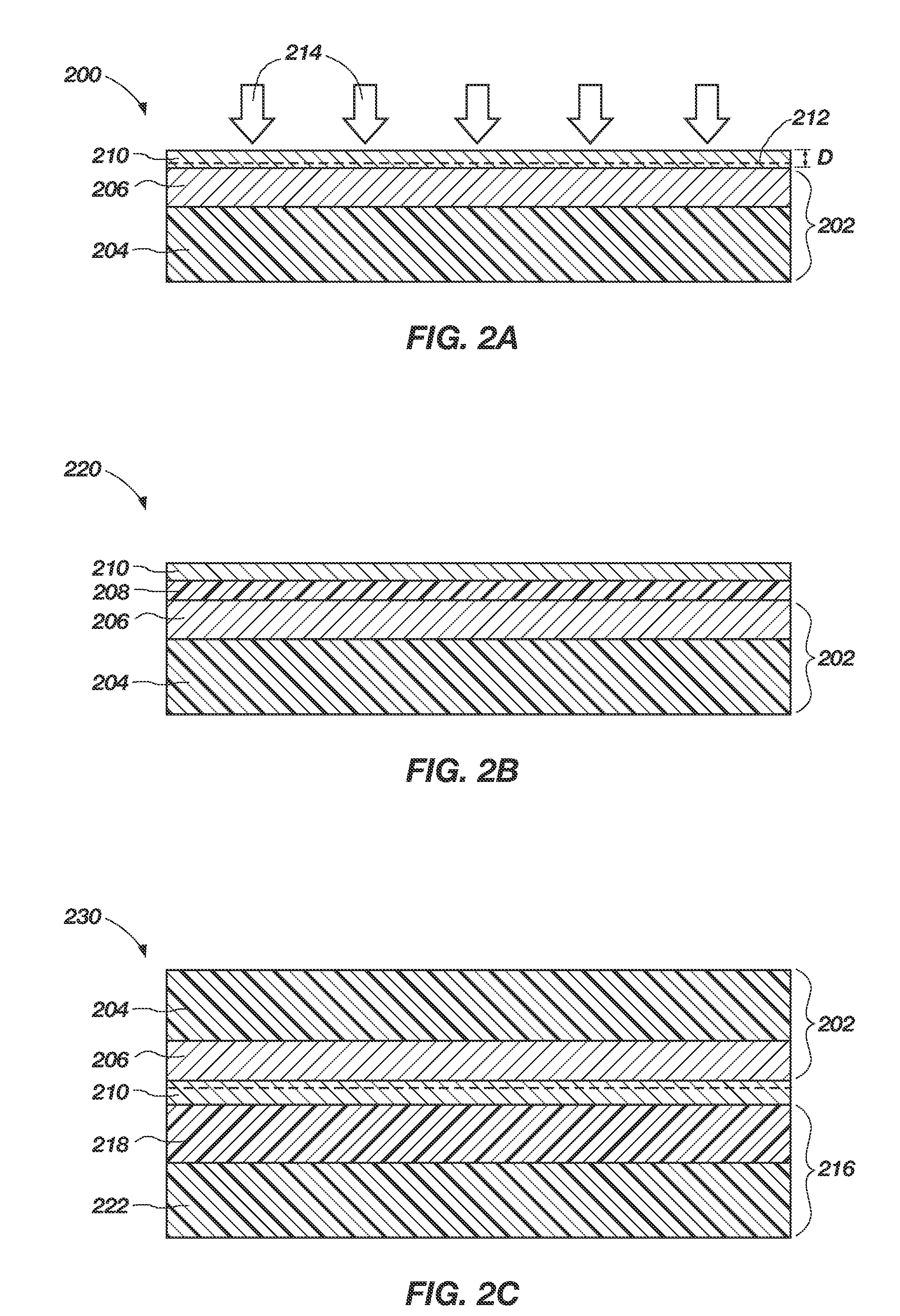
[0026]The illustrations presented herein are not meant to be actual views of any particular material, apparatus, system, or method, but are merely idealized representations which are employed to describe the present invention. Additionally, elements common between figures may retain the same numerical designation.

[0027]As used herein, the term “III-V type semiconductor material” means and includes any material predominantly comprised of one or more elements from group IIIA of the periodic table (B, Al, Ga, In, and Tl) and one or more elements from group VA of the periodic table (N, P, As, Sb, and Bi).

[0028]As used herein, the term “II-VI type semiconductor material” means and includes any material predominantly comprised of one or more elements from group IIB of the periodic table (Zn, Cd, and Hg) and one or more elements from group VIA of the periodic table (O, S, Se, Te, and Po).

[0029]As used herein, the term “critical thickness,” when used with respect to a material, means the ma...


PUM


Abstract

Methods of fabricating semiconductor devices or structures include forming structures of a semiconductor material overlying a layer of a compliant material, subsequently changing the viscosity of the compliant material to relax the semiconductor material structures, and utilizing the relaxed semiconductor material structures as a seed layer in forming a continuous layer of relaxed semiconductor material. In some embodiments, the layer of semiconductor material may comprise a III-V type semiconductor material, such as, for example, indium gallium nitride. Novel intermediate structures are formed during such methods. Engineered substrates include a continuous layer of semiconductor material having a relaxed lattice structure.

Description

CROSS-REFERENCE TO RELATED APPLICATION[0001]This application claims the benefit under 35 U.S.C. §119(e) of U.S. Provisional Application No. 61 / 109,784, filed Oct. 30, 2008, which is incorporated herein by reference.FIELD OF THE INVENTION[0002]The present invention generally relates to the fabrication of semiconductor structures or devices using engineered substrates, to intermediate structures formed during the fabrication of semiconductor structures or devices, and to engineered substrates for use in the fabrication of semiconductor structures or devices.BACKGROUND OF THE INVENTION[0003]Substrates that include one or more layers of semiconductor material are used to form a wide variety of semiconductor structures and devices including, for example, integrated circuit (IC) devices (e.g., logic processors and memory devices), radiation emitting devices (e.g., light emitting diodes (LEDs), resonant cavity light emitting diodes (RCLEDs), vertical cavity surface emitting lasers (VCSELs)...

Claims


Application Information

Patent Timeline
IPC IPC(8): H01L21/20H01L29/20
CPCH01L21/0242H01L21/02458H01L21/0254H01L21/02647H01L21/76254H01L21/02488H01L29/0684H01L29/2003H01L21/20H01L21/786
Inventor ARENA, CHANTAL
Owner S O I TEC SILICON ON INSULATOR THECHNOLOGIES
Why Eureka
Try Eureka