Four junction inverted metamorphic multijunction solar cell

a solar cell and metamorphic technology, applied in the field of semiconductor devices, can solve the problems of increasing the complexity of manufacturing, the number of practical difficulties relating to the appropriate choice of materials and fabrication steps, and the number of difficult material selection and fabrication steps

Active Publication Date: 2010-05-13
SOLAERO TECH CORP
View PDF99 Cites 90 Cited by
  • Summary
  • Abstract
  • Description
  • Claims
  • Application Information

AI Technical Summary

Problems solved by technology

Compared to silicon, III-V compound semiconductor multijunction devices have greater energy conversion efficiencies and generally more radiation resistance, although they tend to be more complex to manufacture.
However, the materials and structures for a number of different layers of the cell proposed and described in such reference present a number of practical difficulties relating to the appropriate choice of materials and fabrication steps.

Method used


Image

  • Four junction inverted metamorphic multijunction solar cell
  • Four junction inverted metamorphic multijunction solar cell
  • Four junction inverted metamorphic multijunction solar cell

Examples


first embodiment

[0106]FIG. 5 is a cross-sectional view of the solar cell of the present invention depicting the semiconductor structure of FIG. 2 bonded with the semiconductor structure of FIG. 4.

[0107]The method of bonding the wafers of the structures of FIG. 2 and FIG. 4 according to the present invention is as follows. The wafers are placed in an ultra high vacuum chamber. The wafers are then exposed to H+ ions at 400° C. to remove all oxides and carbonaceous materials on the bonding surfaces of each wafer. They are then aligned, and are mechanically brought together or compressed to form a bond at near zero pressure. Subsequent processing of the bonded structure will be described below, beginning with the description of FIG. 9.

[0108]Turning to a second embodiment of the present invention, in which the tunnel diode is formed on the second substrate rather than the first substrate, FIG. 6A depicts a cross-sectional view of first a portion of the solar cell in a second embodiment of the present in...

second embodiment

[0115]FIG. 8 is a cross-sectional view of the solar cell of the present invention depicting the substrate of FIG. 6 bonded with the substrate of FIG. 7C.

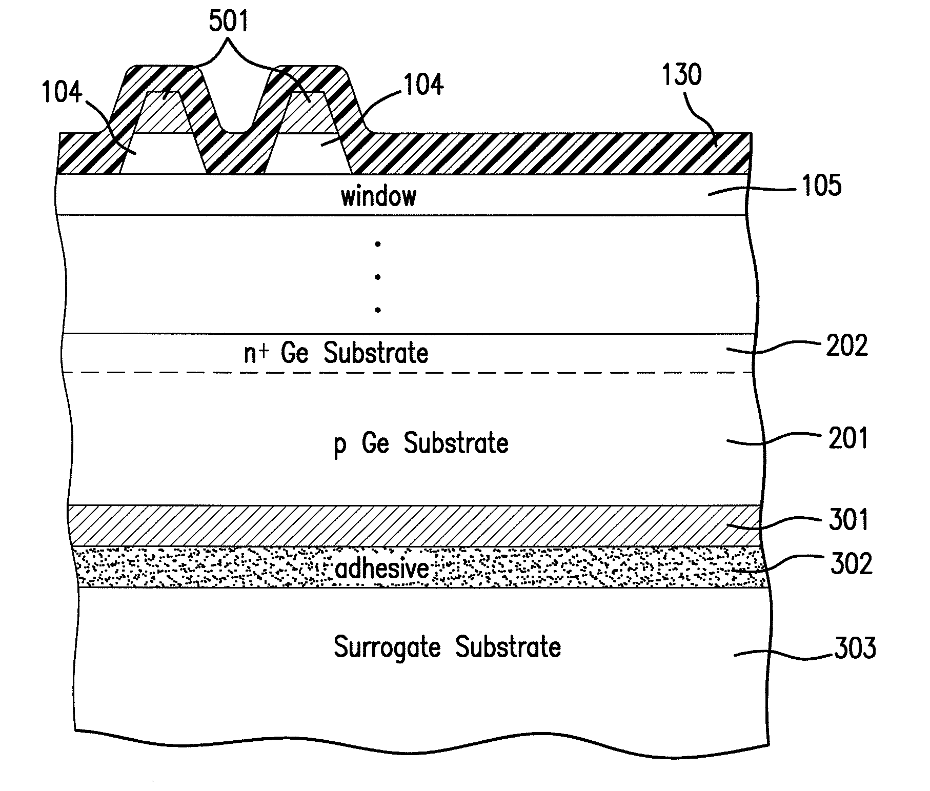
[0116]FIG. 9 is a highly simplified cross-sectional view of the solar cell semiconductor of FIG. 5 or FIG. 8 depicting just a few of the layers (201, 202, and 203) at the top of the semiconductor structure and of few of the layers (105, 104, 103, 102) at the bottom of the structure over the GaAs substrate 101.

[0117]FIG. 10 is a cross-sectional view of the solar cell of FIG. 9 (i.e., a simplified version of FIG. 5 or FIG. 8) after the next process step in which a metal contact layer 301 is deposited over the exposed surface of the germanium substrate 201. The metal is preferably the sequence of metal layers Ti / Au / Ag / Au, although other metal sequences can be used as well.

[0118]FIG. 11A is a cross-sectional view of the structure of FIG. 10 after the next process step in which an adhesive layer 302 is deposited over the metal layer 301....


PUM


Abstract

A method of manufacturing a solar cell by providing a first semiconductor substrate and depositing a first sequence of layers of semiconductor material to form a first solar subcell, including a first bond layer disposed on the top of the first sequence of layers. A second semiconductor substrate is provided, and on the top surface of the second substrate a second sequence of layers of semiconductor material is deposited forming at least a second solar subcell. A second bond layer is disposed on the top of said second sequence of layers. The first solar subcell is mounted on top of the second solar subcell by joining the first bond layer to the second bond layer in an ultra high vacuum chamber, and the first semiconductor substrate is removed.

Description

REFERENCE TO RELATED APPLICATIONS[0001]This application is related to co-pending U.S. patent application Ser. No. 12 / 258,190 filed Oct. 24, 2008.[0002]This application is related to co-pending U.S. patent application Ser. No. 12 / 253,051 filed Oct. 16, 2008.[0003]This application is related to co-pending U.S. patent application Ser. No. 12 / 190,449 filed Aug. 12, 2008.[0004]This application is related to co-pending U.S. patent application Ser. No. 12 / 187,477 filed Aug. 7, 2008.[0005]This application is related to co-pending U.S. patent application Ser. No. 12 / 218,582 filed Jul. 18, 2008.[0006]This application is related to co-pending U.S. patent application Ser. No. 12 / 218,558 filed Jul. 17, 2008.[0007]This application is related to co-pending U.S. patent application Ser. No. 12 / 123,864 filed May 20, 2008.[0008]This application is related to co-pending U.S. patent application Ser. No. 12 / 102,550 filed Apr. 14, 2008.[0009]This application is related to co-pending U.S. patent applicatio...

Claims


Application Information

Patent Timeline
Patent Type & Authority Applications(United States)
IPC IPC(8): H01L31/00H01L21/02
CPCH01L31/06875H01L31/078H01L31/18Y02E10/544Y02P70/521Y02P70/50
Inventor CORNFELD, ARTHUR
Owner SOLAERO TECH CORP
Why Eureka
Try Eureka