Semiconductor integrated circuit and control method for clock signal synchronization

a technology of integrated circuits and clock signals, which is applied in the direction of generating/distributing signals, instruments, sustainable buildings, etc., can solve the problems of long time consumption of changing the power supply voltage, difficult to increase the difference between operating voltages to be varied, and increase an area, so as to maximize the low power consumption effect of dvfs control, consume long time, and degrade performance

Inactive Publication Date: 2010-05-13
RENESAS ELECTRONICS CORP
View PDF7 Cites 32 Cited by
  • Summary
  • Abstract
  • Description
  • Claims
  • Application Information

AI Technical Summary

Benefits of technology

[0011]Low-voltage control needs to be used actively so as to maximize the low power consumption effect of the DVFS control. In this case, changing the power-supply voltage consumes long time due to small power-supply impedance. Operations need to be inactive during this period so as to ensure the synchronization, greatly degrading the performance. Accordingly, the DVFS control requires to minimize a period for inactivating the system. The DVFS control improves the low power consumption effect as a voltage difference increases. However, the inventors found that the known examples described in Non-patent Documents 1 and 2 make it difficult to increase a difference between operating voltages to be varied. Increasing an operating voltage difference, if possible, may increase an area and degrade the comparison precision.

Problems solved by technology

In this case, changing the power-supply voltage consumes long time due to small power-supply impedance.
However, the inventors found that the known examples described in Non-patent Documents 1 and 2 make it difficult to increase a difference between operating voltages to be varied.
Increasing an operating voltage difference, if possible, may increase an area and degrade the comparison precision.

Method used


Image

  • Semiconductor integrated circuit and control method for clock signal synchronization
  • Semiconductor integrated circuit and control method for clock signal synchronization
  • Semiconductor integrated circuit and control method for clock signal synchronization

Examples


Embodiment Construction

1. Summary of the preferred embodiments

[0047]The following provides a summary of the preferred embodiments of the invention disclosed in this specification. The summary of the preferred embodiments contains parenthesized reference numerals with reference to the drawings. The reference numerals just show examples belonging to the concept of the components to which the reference numerals are assigned.

[0048] (Cooperation with Power Supplying LSI)

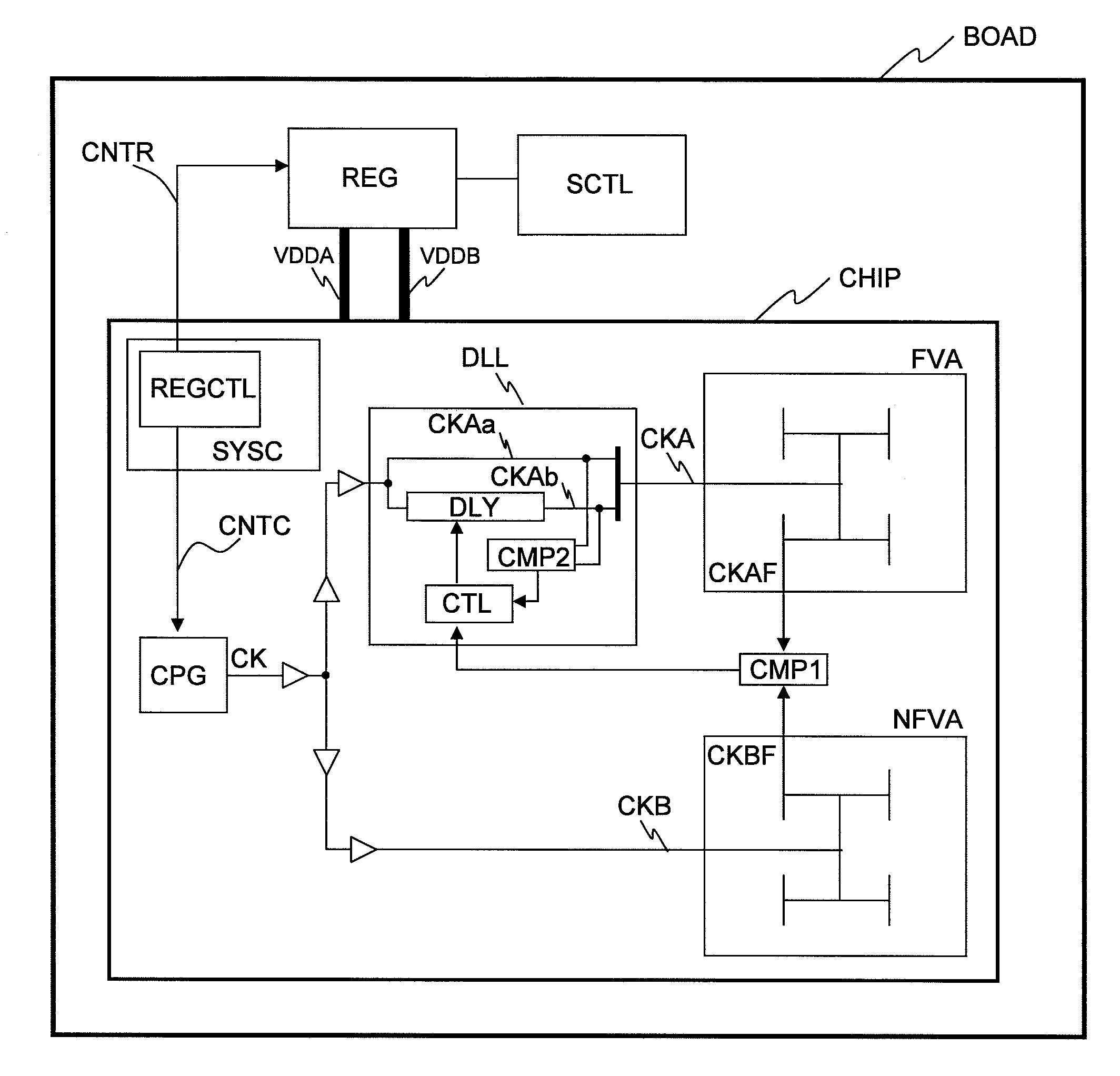
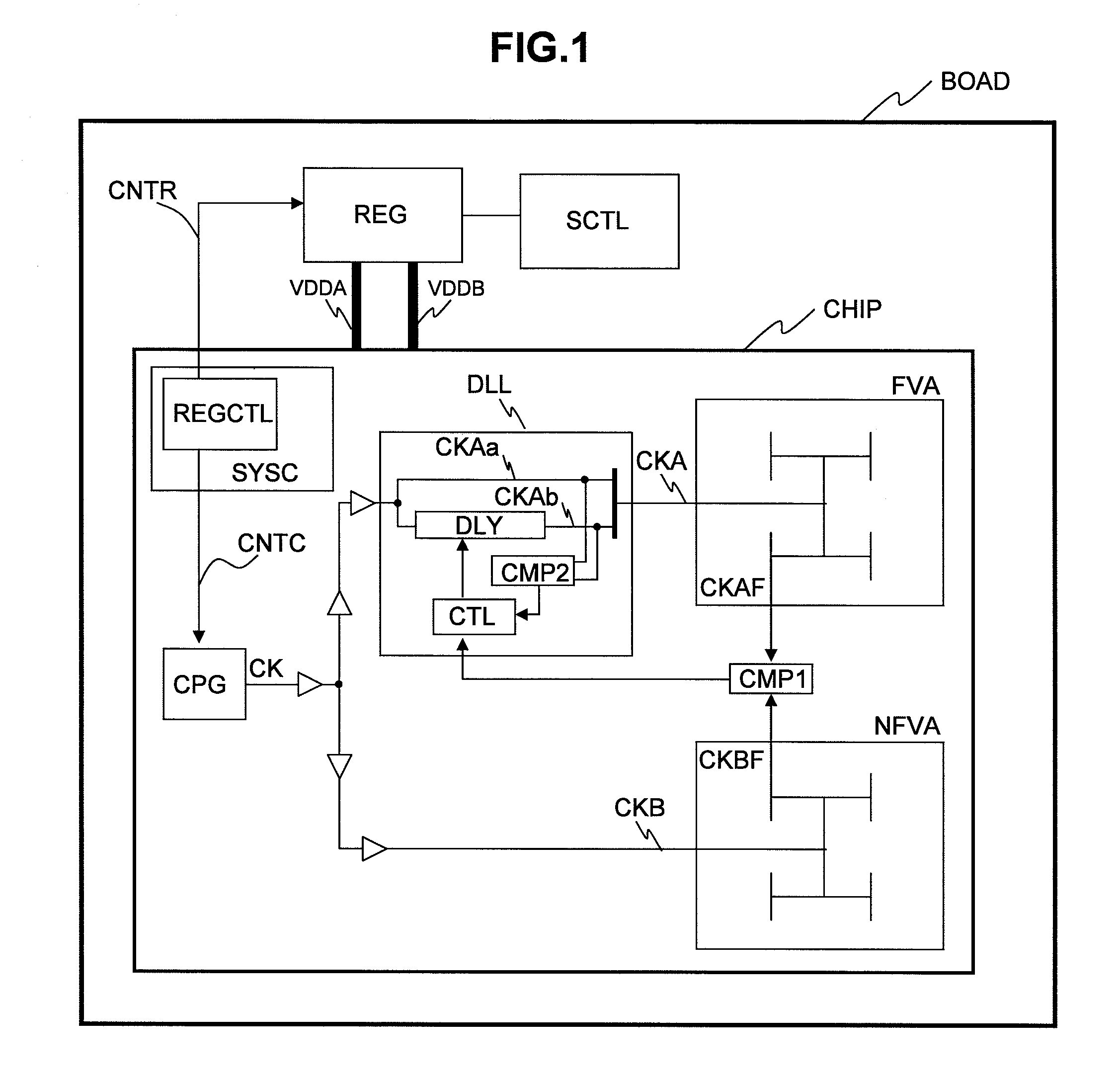
[0049]A semiconductor integrated circuit according to the invention includes: a first circuit that operates using a first power-supply voltage supplied from a power supplying LSI; a second circuit that operates using a second power-supply voltage; a clock generation circuit that generates a clock signal; a clock tree that transmits a clock generated by the clock generation circuit to the first circuit and the second circuit; a clock synchronization circuit having a plurality of delay stages that perform clock delay adjustment between a path for...


PUM


Abstract

There is a need to ensure operation performance of a circuit region under DVFS control at low costs and highly precisely while a power-supply voltage change is made to the region. A first circuit (FVA) uses a first power-supply voltage (VDDA) for operation. A second circuit (NFVA) uses a second power-supply voltage (VDDB) for operation. A clock delay may be adjusted between paths for transmitting a clock to these circuits. When VDDA equals VDDB, a clock is distributed to FVA through a path that does not contain a delay device for phase adjustment. When the power-supply voltage for the FVA region is reduced, a clock is distributed to the FVA region based on a phase equivalent to one or two cycles of the clock displaced. Synchronization control is provided to synchronize clocks (CKAF and CKBF) and ensures operation so that a phase of two clocks to be compared fits in a range of design values while the power-supply voltage for the first circuit is changed.

Description

CLAIM OF PRIORITY[0001]The present application claims priority from Japanese patent application JP 2008-288836 filed on Nov. 11, 2008, the content of which is hereby incorporated by reference into this application.FIELD OF THE INVENTION[0002]The present invention relates to a clock signal synchronization technology for semiconductor integrated circuits. More particularly, the invention relates to a technology usefully applicable to not only system LSI and microprocessors for portable devices but also DVFS control in data processing systems, for example.BACKGROUND OF THE INVENTION[0003]Decreasing a power-supply voltage effectively reduces power consumption of a semiconductor integrated circuit. This is because power consumption of a transistor included in a semiconductor can be reduced in proportion to the square of the power-supply voltage. Further, a switching operation speed (operating frequency) of the transistor is approximately proportional to the power-supply voltage. There ma...

Claims


Application Information

Patent Timeline
Patent Type & Authority Applications(United States)
IPC IPC(8): H03L7/06
CPCG06F1/10G06F1/3203G06F1/324G06F1/3296H03L7/0818H03L7/089Y02B60/1217Y02B60/1285H03L7/0814H03L7/0816Y02D10/00
Inventor KANNO, YUSUKESAEN, MAKOTOKOMATSU, SHIGENOBUONOUCHI, MASAFUMI
Owner RENESAS ELECTRONICS CORP
Why Eureka
Try Eureka