Heterogeneous GeSn-based silicon-based deep groove protection PiN diode and production method thereof

A diode and deep groove technology, applied in the field of heterogeneous GeSn-based silicon-based deep groove protection PiN diodes and its preparation, can solve the disadvantages of silicon-based highly integrated reconfigurable antenna miniaturization, low power consumption, poor distribution uniformity, concentration Low-level problems, to achieve the effect of improving antenna system integration and stealth performance, good device performance, and improving low power consumption performance

Pending Publication Date: 2021-06-18
ENG UNIV OF THE CHINESE PEOPLES ARMED POLICE FORCE
View PDF3 Cites 0 Cited by
  • Summary
  • Abstract
  • Description
  • Claims
  • Application Information

AI Technical Summary

Problems solved by technology

However, due to the disadvantages of low solid-state plasma concentration and poor distribution uniformity in the traditional PiN diode, the power consumption of the diode can reach about 0.2W during normal operation. When multiple diodes are connected in series to form an array, the overall power consumption will be very large. , which is not conducive to the development of silicon-based highly integrated reconfigurable antennas in the direction of miniaturization and low power consumption

Method used


Image

  • Heterogeneous GeSn-based silicon-based deep groove protection PiN diode and production method thereof
  • Heterogeneous GeSn-based silicon-based deep groove protection PiN diode and production method thereof
  • Heterogeneous GeSn-based silicon-based deep groove protection PiN diode and production method thereof

Examples


Embodiment 1

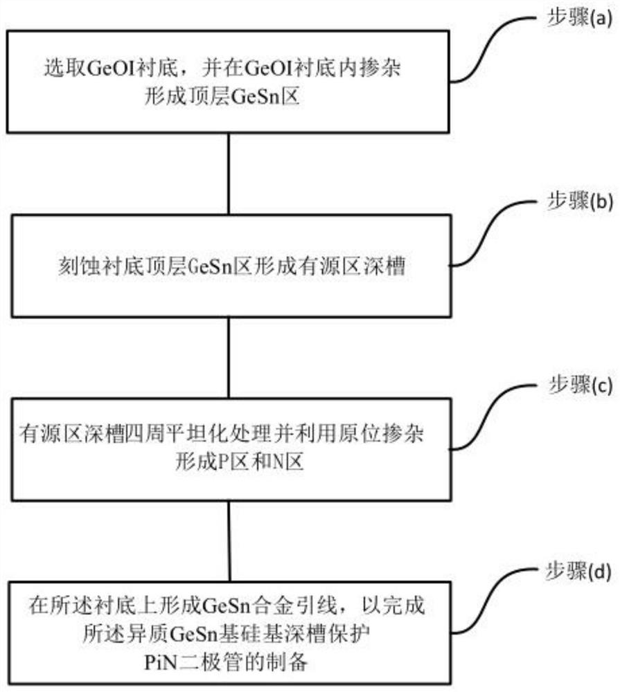
[0051] See figure 1 , figure 1 It is a flow chart of a method for preparing a heterogeneous GeSn-based silicon-based deep trench protected PiN diode according to an embodiment of the present invention. The method is suitable for preparing a heterogeneous GeSn-based silicon-based deep trench protected PiN diode, and the diode is mainly used for making silicon Base height integrated reconfigurable antenna. The method comprises the steps of:

[0052] (a) select a GeOI substrate, and dope in the GeOI substrate to form a top GeSn region;

[0053] (b) etching the GeSn region on the top layer of the substrate to form a deep groove in the active region;

[0054] (c) planarizing the sidewalls around the deep trench in the active region and using in-situ doping to form P and N regions;

[0055] (d) forming a GeSn alloy lead on the substrate to complete the preparation of the heterogeneous GeSn-based silicon-based deep groove protection PiN diode.

[0056] Wherein, for step (a), the...

Embodiment 2

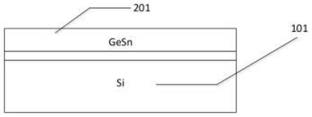
[0093] See Figure 2a-Figure 2s , Figure 2a-Figure 2s It is a schematic diagram of a preparation method of a heterogeneous GeSn-based silicon-based deep groove protection PiN diode according to an embodiment of the present invention. On the basis of the above-mentioned embodiment 1, a heterogeneous GeSn-based silicon-based deep trench with a solid-state plasma region length of 80 microns is prepared. The groove protection PiN diode is taken as an example to describe in detail. The length of the solid-state plasma region can be between 50 microns and 150 microns. The specific steps are as follows:

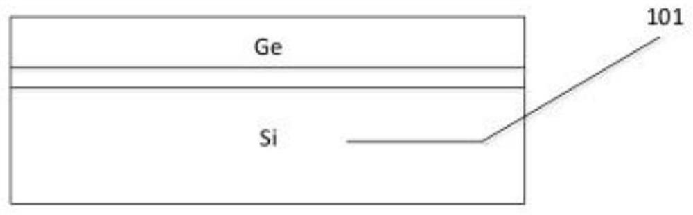
[0094] S10, selecting a GeOI substrate.

[0095] See Figure 2a , the crystal orientation of the GeOI substrate 101 may be (100) or (110) or (111), without any limitation here. In addition, the doping type of the GeOI substrate 101 can be n-type or p-type, and the doping concentration is, for example, 0.5×10 14 ~1×10 15 cm -3 , the thickness of the top layer Ge is, for exampl...

Embodiment 3

[0133] Please refer to image 3 , image 3 It is a schematic diagram of a device structure of a heterogeneous GeSn-based silicon-based deep trench protection PiN diode according to an embodiment of the present invention. The heterogeneous GeSn-based silicon-based deep trench protection PiN diode adopts the above-mentioned figure 1 prepared as indicated. Specifically, the heterogeneous GeSn-based silicon-based deep groove protection PiN diode is prepared and formed on the GeOI substrate 301, and the P region 303, the N region 304 of the diode, and the local area between the P region 303 and the N region 304 in the lateral direction. The constitutive regions are located in the GeSn region 302 of the top layer of the GeOI substrate.

[0134] The present invention provides a heterogeneous GeSn-based silicon-based deep trench protection PiN diode. By introducing deep trench isolation technology and Si-GeSn-Si heterostructure, the low power consumption performance of the diode is...


PUM

PropertyMeasurementUnit
lengthaaaaaaaaaa
thicknessaaaaaaaaaa

Abstract

The invention relates to a heterogeneous GeSn-based silicon-based deep groove protection PiN diode and a production method thereof. The production method comprises the steps: selecting a GeOI substrate, and carrying out the doping in the GeOI substrate, and forming a top layer GeSn region; etching the GeSn region on the top layer of the substrate to form an active region deep groove; flattening the periphery of the deep groove in the active region and forming a P region and an N region by using in-situ doping; and forming a GeSn alloy lead on the substrate so as to complete the production of the heterogeneous GeSn-based silicon-based deep groove protection PiN diode. By introducing a deep groove isolation process and a Si-GeSn-Si heterostructure, the low power consumption performance of the diode is greatly improved, and the power consumption of the PiN diode can be reduced by one order of magnitude.

Description

technical field [0001] The invention relates to the technical field of semiconductor materials and device manufacturing, in particular to a heterogeneous GeSn-based silicon-based deep groove protection PiN diode and a preparation method thereof. Background technique [0002] Modern communication systems have increasingly strong requirements for miniaturization and integration. Antennas as electromagnetic radiation and receiving devices in communication systems play an important role in system performance metrics. This requires antennas to achieve multi-directional polarization, On the basis of multiple working frequency bands and multiple application functions, the complexity of the antenna system is reduced for easy operation, the weight and physical size of the antenna system are reduced, and the combination with modern semiconductor manufacturing processes promotes the development of communication systems in the direction of miniaturization and integration. The preparatio...

Claims


Application Information

Patent Timeline
Patent Type & Authority Applications(China)
IPC IPC(8): H01L29/868H01L29/06H01L21/329
CPCH01L29/868H01L29/0603H01L29/0684H01L29/6609
Inventor 苏汉王华剑
Owner ENG UNIV OF THE CHINESE PEOPLES ARMED POLICE FORCE
Why Eureka
Try Eureka