Memory device and writing method thereof

a memory device and writing method technology, applied in information storage, static storage, digital storage, etc., can solve the problem of long write time, and achieve the effect of shortening the write time of the selected memory cell and quick driving the bit lin

Inactive Publication Date: 2010-05-20
LONGITUDE SEMICON S A R L
View PDF9 Cites 11 Cited by
  • Summary
  • Abstract
  • Description
  • Claims
  • Application Information

AI Technical Summary

Benefits of technology

[0011]According to this invention, by providing a write amplifier adapted to drive a bit line, connected to a selected phase change memory cell, with a first current driving capability and then to drive the bit line to a write voltage, corresponding to data to be written, with a second current driving capability lower than the first current driving capability, it is possible to quickly drive the bit line to the required voltage and thus to shorten the write time for the selected memory cell.

Problems solved by technology

The present inventors have discovered that when driving a bit line, it takes time to raise the voltage of the bit line to a predetermined value due to a relatively large capacitance of the bit line, thus resulting in a long write time.

Method used


Image

  • Memory device and writing method thereof
  • Memory device and writing method thereof
  • Memory device and writing method thereof

Examples


first embodiment

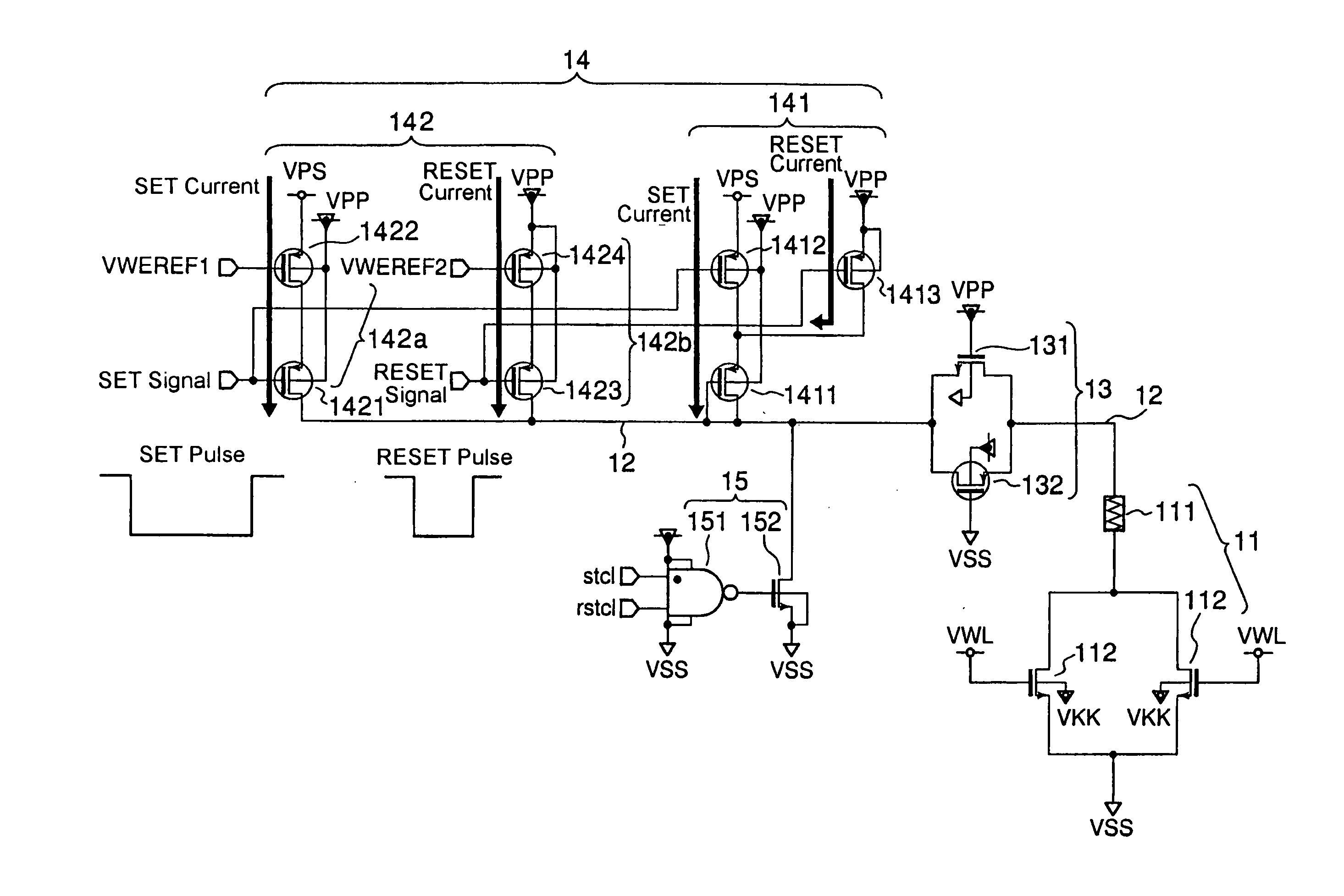
[0019]FIG. 1 is a circuit diagram showing a main portion of a phase change memory device (or a semiconductor device) according to this invention. FIG. 1 only illustrates a single memory cell 11 and a portion relating to a write operation for this memory cell 11. Actually, the phase change memory device includes a plurality of memory cells arranged in rows and columns. Hereinafter, it is assumed that the memory cell 11 is a selected memory cell in which data are written.

[0020]The phase change memory device of FIG. 1 comprises a cell array (not illustrated) including the memory cell 11, Yj switches (bit line selection switches) 13 for hierarchizing bit lines 12 of the cell array, respectively, write amplifiers (write drivers) 14 for driving the bit lines 12 selected by the Yj switches 13, respectively, and voltage drop circuits 15 each for dropping the voltage of the corresponding bit line 12 to a low-potential side power supply VSS level. In this specification, a “bit line” includes ...

second embodiment

[0044]Referring now to FIG. 4, a phase change memory device (or a semiconductor device) according to this invention will be described.

[0045]The phase change memory device of FIG. 4 differs from that of FIG. 1 in that a write amplifier 41 is used instead of the write amplifier 14.

[0046]The write amplifier 41 comprises a SET write amplifier section 41a and a RESET write amplifier section 41b.

[0047]The SET write amplifier section 41a has a switching PMOS 411 and a current trimming PMOS 412 connected in series between a bit line 12 and a high-potential side power supply VPS. Further, the SET write amplifier section 41a has a control voltage changing section 413 for controlling the control voltage of the current trimming PMOS 412. The control voltage changing section 413 comprises a delay circuit 4131, and a PMOS 4132 and an NMOS 4133 each adapted to be turned on or off according to an output from the delay circuit 4131.

[0048]A SET signal stcl is input, as an input signal, to the gate o...


PUM


Abstract

A write amplifier for driving a bit line connected to a selected phase change memory cell drives the bit line with a first current driving capability and then drives the bit line with a second current driving capability lower than the first current driving capability.

Description

[0001]This application is based on and claims priority from Japanese Patent Application No. 2008-296848 filed on Nov. 20, 2008. The disclosure thereof is incorporated herein by reference in its entirety.BACKGROUND OF THE INVENTION[0002]1. Field of the Invention[0003]This invention relates to a memory device and a writing method thereof.[0004]2. Description of the Related Art[0005]The phase state of a phase change material such as chalcogenide can be changed between a crystalline state and an amorphous state by heating and cooling and the phase change material exhibits a different resistance value depending on its phase state. A memory device configured to store information using such a phase change material (variable resistance element) is called a phase change memory device.[0006]In the phase change memory device, the phase state of the variable resistance element is changed by controlling the magnitude and duration of current supplied to the variable resistance element to heat and...

Claims


Application Information

Patent Timeline
Patent Type & Authority Applications(United States)
IPC IPC(8): G11C11/00G11C8/08G11C7/00
CPCG11C7/1078G11C7/1096G11C2013/0078G11C13/0069G11C13/0004
Inventor SATO, KOJINAKAI, KIYOSHIMAE, KENJI
Owner LONGITUDE SEMICON S A R L
Why Eureka
Try Eureka