Nonvolatile Memory Device with Incremental Step Pulse Programming

a non-volatile memory and programming technology, applied in static storage, digital storage, instruments, etc., can solve the problems of reducing the time required to update the write buffer, and reducing the programming tim

Active Publication Date: 2010-05-20
SAMSUNG ELECTRONICS CO LTD
View PDF3 Cites 31 Cited by
  • Summary
  • Abstract
  • Description
  • Claims
  • Application Information

AI Technical Summary

Benefits of technology

[0008]The inventive concept provides a nonvolatile memory device which may shorten the programming time by decreasing the time to verify whether a memory cell is programmed or not.

Problems solved by technology

Volatile memory devices are generally characterized by fast data access and write speeds, but lose stored data in the absence of applied power.
In contrast, non-volatile memory devices generally provide slower data access and write speeds but retain stored data in the absence of applied power.
Accordingly, when the verification of the memory cell is performed, a relatively large of time is needed to update the write buffer with data that is read by the sense amplifier.

Method used


Image

  • Nonvolatile Memory Device with Incremental Step Pulse Programming
  • Nonvolatile Memory Device with Incremental Step Pulse Programming
  • Nonvolatile Memory Device with Incremental Step Pulse Programming

Examples


Embodiment Construction

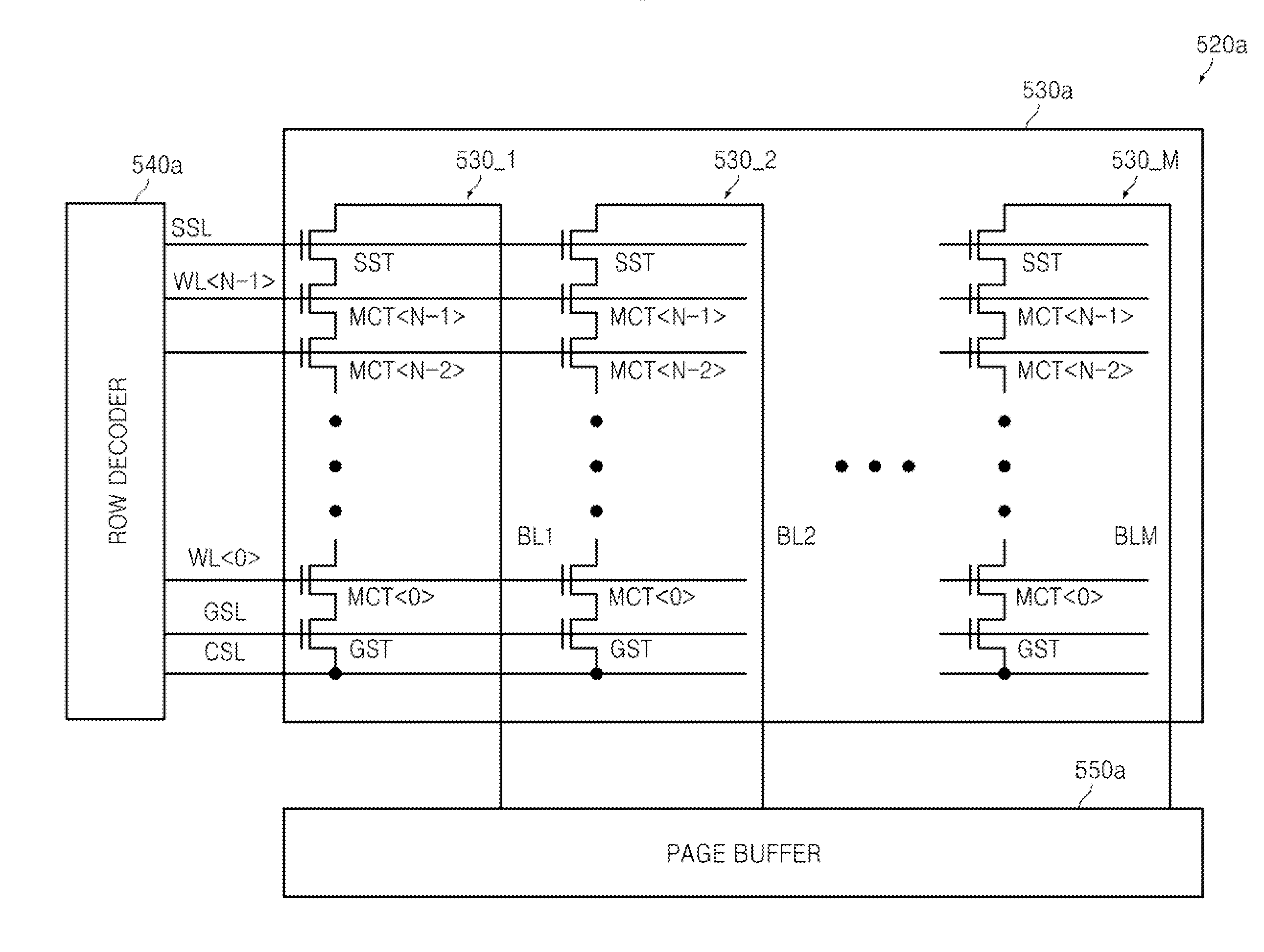
[0025]The attached drawings illustrate exemplary embodiments of the present inventive concept. Hereinafter, exemplary embodiments of the present inventive concept are explained with reference to the attached drawings. Like reference numerals in the drawings may denote like elements.

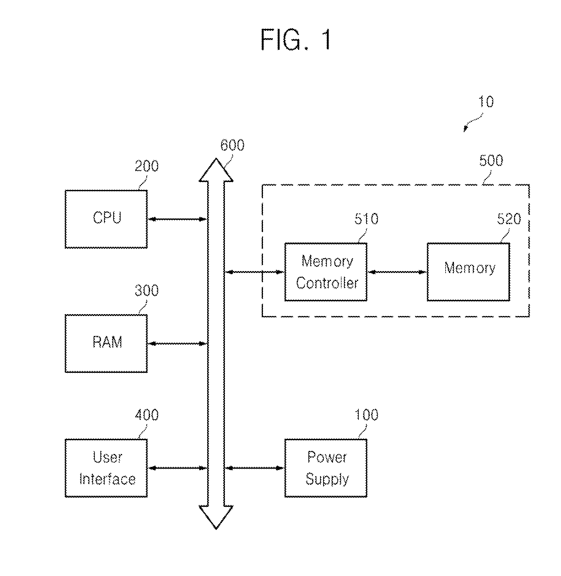
[0026]FIG. 1 is a block diagram of an electronic system 10 according to an exemplary embodiment of the present inventive concept. In FIG. 1, the electronic system 10 may be a system such as a mobile device, a laptop computer, or a desktop computer. Referring to FIG. 1, the electronic system 10 according to the present exemplary embodiment may include a nonvolatile memory system 500, a power supply 100, a central processing unit (CPU) 200, a RAM 300, a user interface 400, and a system bus 600 electrically connecting these elements.

[0027]The CPU 200 controls the overall operation of the electronic system 10. The RAM 300 stores information needed for the operation of the electronic system 10. The RAM 300 is ...


PUM


Abstract

A nonvolatile memory device includes a sense amplifier circuit sensing first data from a memory cell via a bit line and outputting the sensed first data, in response to a read command. A write driver circuit programs the memory cell and stores second data indicating a programming state of the memory cell, in response to a program command. A verification block outputs a result of a comparison between the first and second data in response to a first read command. The second data is updated based on the determination on the programming of the memory cell in response to a second read command applied following the first read command.

Description

CROSS-REFERENCE TO RELATED APPLICATIONS[0001]This application claims priority to Korean Patent Application No. 10-2008-0115151, filed on Nov. 19, 2008, in the Korean Intellectual Property Office, the disclosure of which is incorporated herein in its entirety by reference.BACKGROUND[0002]1. Technical Field[0003]The inventive concept relates to a nonvolatile memory device, and more particularly, to a nonvolatile memory device performing a programming operation according to incremental step pulse programming (ISPP).[0004]2. Discussion of the Related Art[0005]Semiconductor memory devices (hereafter, “memory devices”) include volatile memory devices and non-volatile memory devices. Volatile memory devices are generally characterized by fast data access and write speeds, but lose stored data in the absence of applied power. In contrast, non-volatile memory devices generally provide slower data access and write speeds but retain stored data in the absence of applied power. Examples of nonv...

Claims


Application Information

Patent Timeline
Patent Type & Authority Applications(United States)
IPC IPC(8): G11C16/04G11C16/06
CPCG11C16/3459G11C16/3454G11C16/26G11C16/34
Inventor LEE, SEUNG WON
Owner SAMSUNG ELECTRONICS CO LTD
Why Eureka
Try Eureka